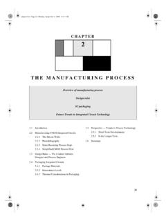
Transcription of Lecture11-MOS Cap Delay
1 EE1411 EECS1411 Lecture #11EE141EE141--Fall 2010 Fall 2010 Digital Integrated Digital Integrated CircuitsCircuitsLecture 11 Lecture 11 MOS Capacitance MOS Capacitance and Delayand DelayEE1412 EECS1412 Lecture #11 AnnouncementsAnnouncements No lab Fri., Mon. Labs restart next week Midterm #1 Thurs. Oct. 7th, 6:30-8:00pm Exam is open notes, book, calculators, #11 Class MaterialClass Material Last lecture Using the MOS model: Inverter VTC Today s lecture MOS Capacitance Using the MOS Model: Delay Reading ( , )EE1414 EECS1414 Lecture #11 MOS CapacitanceMOS CapacitanceEE1415 EECS1415 Lecture #11 CGDCGSCSBCDBCGBMOS CapacitancesMOS Capacitances= CGCS+ CGSO= CGCD+ CGDO= CGCB= CdiffGSDB= CdiffEE1416 EECS1416 Lecture #11 Gate CapacitanceGate Capacitance Capacitance (per area)
2 From gate across the oxide is W L Cox, where Cox= ox/toxEE1417 EECS1417 Lecture #11 Gate CapacitanceGate Capacitance Distribution between terminals is complex Capacitance is really distributed Useful models lump it to the terminals Several operating regions: Way off, off, transistor linear, transistor saturatedEE1418 EECS1418 Lecture #11 Transistor In CutoffTransistor In Cutoff When the transistor is off, no carriers in channel to form the other side of the capacitor. Substrate acts as the other capacitor terminal Capacitance becomes series combination of gate oxide and depletion capacitance L S D W G C OL C GB C OL C jSB C jDB j x EE1419 EECS1419 Lecture #11 Transistor In Cutoff Transistor In Cutoff (cont(cont d)d) When |VGS| < |VT|, total CGCB much smaller than W L Cox Usually just approximate with CGCB= 0 in this region.
3 (If VGSis very negative (for NMOS), depletion region shrinks and CGCB goes back to ~W L Cox) L S D W G C OL C GB C OL C jSB C jDB j x EE14110 EECS14110 Lecture #11 Transistor in Linear RegionTransistor in Linear Region Channel is formed and acts as the other terminal CGCB drops to zero (shielded by channel) Model by splitting oxide cap equally between source and drain Changing either voltage changes the channel charge L SD WG COLC G C OL C JC CjSBC jDB LDj x EE14111 EECS14111 Lecture #11 Transistor in Saturation RegionTransistor in Saturation Region Changing source voltage doesn t change VGCuniformly VGCat pinch off point still VTH Bottom line.
4 CGCS 2/3 W L Cox L SDWGCOLC G COL CJC CjSBCjDB LDj x EE14112 EECS14112 Lecture #11 Transistor in Saturation Region Transistor in Saturation Region (cont(cont d)d) Drain voltage no longer affects channel charge Set by source and VDS_sat If change in charge is 0, CGCD= 0 L SDWGCOLC G COL CJC CjSBCjDB LDj x EE14113 EECS14113 Lecture #11 Gate CapacitanceGate CapacitanceCgatevs. VGS(with VDS= 0)Cgatevs. operating regionEE14114 EECS14114 Lecture #11 Gate Overlap CapacitanceGate Overlap CapacitancedoxOxCC =xdxdLdPolysilicon gateTop viewGate-bulkoverlapSourcen+Drainn+Wxdxd LdPolysilicon gateTop viewGate-bulkoverlapSourcen+Drainn+WOff/ Lin/Sat CGSO= CGDO= CO Wtoxn+n+Cross sectionLGate oxidetoxn+n+Cross sectionLGate oxideEE14115 EECS14115 Lecture #11 Gate Fringe CapacitanceGate Fringe Capacitance COV not just from metallurgic overlap get fringing fields too Typical value.
5 ~ W(in m)/edgen+n+Cross sectionn+n+Cross sectionFringing fieldsEE14116 EECS14116 Lecture #11 Diffusion CapacitanceDiffusion CapacitanceBottomSide wallSide wallChannelSourceSubstrateWNA+NALSNDxj Bottom Area cap Cbottom= Cj LS W Sidewalls Perimeter cap Csw= Cjsw (2LS+W) GateEdge Cge= Cjgate W Usually automatically included in the SPICE modelEE14117 EECS14117 Lecture #11 Junction Capacitance (2)Junction Capacitance (2) SPICE model equations: Area CJ= area CJ0/ (1+ |VDB|/ )mj Perimeter CJ= perim CJSW/ (1 + |VDB|/ )mjsw Gate edge CJ= W CJgate/ (1 + |VDB|/ )mjswg How do we deal with nonlinear capacitance?
6 Voltage (V)Capacitance [arbitrary units]N+ junction areaN+ junction perimeterP+ junction areaP+ junction perimeter Junction caps are nonlinear CJis a function of junction biasEE14118 EECS14118 Lecture #11 LinearizingLinearizingthe Junction Capacitancethe Junction CapacitanceReplace non-linear capacitance bylarge-signal equivalent linear capacitancewhich displaces equal charge over voltage swing of interestEE14119 EECS14119 Lecture #11 Capacitance Model SummaryCapacitance Model Summary Gate-Channel Capacitance CGC 0(|VGS| < |VT|) CGC= Cox W Leff(Linear) 50% G to S, 50% G to D CGC= (2/3) Cox W Leff(Saturation) 100% G to S Gate Overlap Capacitance CGSO= CGDO= CO W(Always) Junction/Diffusion Capacitance Cdiff= Cj LS W + Cjsw (2LS+ W) + CjgW(Always)EE14120 EECS14120 Lecture #11 Capacitances in Capacitances in m CMOS m CMOS ProcessProcessEE14121 EECS14121 Lecture #11 Simplified ModelSimplified Model Capacitance models important for analysis and intuition But often need something simpler to work with Simple switch model.
7 Lump together as effective linear capacitance to (ac) ground In most processes: CG= CD= 2fF W( m)VoutVinCLVoutVinEE14122 EECS14122 Lecture #11 Model CalibrationModel Calibration--CapacitanceCapacitance Can calculate Cg, Cdbased on tech. parameters But these models are simplified too Another approach: Tune ( , in spice) the linear capacitance until it makes the simplified circuit match the real circuit Matching could be for Delay , power, #11 Model CalibrationModel Calibrationfor Delayfor Delay For gate capacitance: Make inverter fanout 4 Adjust Cloaduntil Delay1 = Delay2 For diffusion capacitance Replace inverter A with a diffusion capacitance loadCloadDelay1 ADelay2 MatchEE14124 EECS14124 Lecture #11 Delay CalibrationDelay Calibration Why did we need that last inverter stage?
8 1 Delay41664"Edge Shaper"Load???EE14125 EECS14125 Lecture #11 The Miller EffectThe Miller EffectVinM1 Cgd1 Vout V V As Vinincreases, Voutdrops Once get into the transition region, gain from Vinto Vout> 1 So, Cgdexperiences voltage swing larger than Vin Which means you need to provide more charge Makes Cgdlook larger than it really is Known as the Miller Effect in the analog worldEE14126 EECS14126 Lecture #11 CMOS CMOS Switching DelaySwitching DelayEE14127 EECS14127 Lecture #11 MOS Transistor as a Switch MOS Transistor as a Switch We modeled this with.
9 ()DSDDvii=dtdVCiDSD=C Discharging a capacitorCRtp= ln (2) RCEE14128 EECS14128 Lecture #11 MOS Transistor as a SwitchMOS Transistor as a Switch Saw that real transistors aren t exactly resistors Look more like current sources in saturation Two questions: Which region of IV curve determines Delay ? How can that match up with the RC model?EE14129 EECS14129 Lecture #11 Transistor Driving a CapacitorTransistor Driving a Capacitor With a step input:IDVDSVDDVDD /2 VGS = VDDVDD VDD/2 VVSAT Transistor is in (velocity) saturation during entire transitionfrom VDDto VDD/2EE14130 EECS14130 Lecture #11 Switching DelaySwitching Delay In saturation, transistor basically acts like a current source.
10 IDSATCVOUTVOUT= VDD-(IDSAT/C)tVOUTtVDDVDD/2tptp= C(VDD/2)/IDSATEE14131 EECS14131 Lecture #11 Switching Delay Switching Delay (with Output Conductance)(with Output Conductance)()()11 +eDSAT-t C IOUTDDV=V - Including output conductance:IDSATCVOUT1/( IDSAT)()()21p +DDDDDSATCVt VI For small :EE14132 EECS14132 Lecture #11RC ModelRC Model Transistor current not linear on VOUT how is the RCmodel going to work? Look at waveforms: Voltage looks like a ramp for RC VOUTNMOSRCEE14133 EECS14133 Lecture #11 Finding Finding ReqReq()()(),21ppRC+DDeqDDDSATt=tCVRC VI=ln 2()()()21=+DDeqDDDSATVR VIln 2 Match the Delay of the RC model with the actual Delay : Often just: ()1 DDeqDSATVRI2ln2 Note that the book uses a different method and VDD/IDSAT instead of ~ VDD/IDSAT.