MOSFET Device Physics and Operation
THE MOS CAPACITOR 5 where V th is the thermal voltage, N a is the shallow acceptor density in the p-type semicon- ductor and n i is the intrinsic carrier density of silicon. According to the usual definition, strong inversion is reached when the total band bending equals 2qϕ b, corresponding to the surface potential ψ s = 2ϕ b.
Download MOSFET Device Physics and Operation

Information
Domain:
Source:
Link to this page:
Documents from same domain
MOSFET Device Physics and Operation
homepages.rpi.edu1 MOSFET Device Physics and Operation 1.1 INTRODUCTION A field effect transistor (FET) operates as a conducting semiconductor channel with two ohmic contacts – the source and the drain – where the number of charge carriers in the
FTIR and DSC of polymer films used for packaging: …
homepages.rpi.edu2 Samples: The pictures of the polymeric material samples that we used in this experiment are shown in figure 1. These samples are used in …
Advances in Radiation Detection and Measurement
homepages.rpi.edu506 Transactions of the American Nuclear Society, Vol. 113, Washington, D.C., November 8–12, 2015 Advances in Radiation Detection and Measurement

Industrial Growth and Competition
homepages.rpi.eduIndustrial Growth and Competition K. Simons, 2003 3 5. Sources of Invention: Big Firms & Streamlined Structure, Improvement & Efficiency.....48

Introduction to Stochastic Processes MATH 6790 | Fall 2008
homepages.rpi.eduKarlin and Taylor, A First Course in Stochastic Processes, Second Edition: A rather advanced textbook with many interesting examples and a rather thorough theoretical development of …

Stock Rocker Vs Roller Rocker
homepages.rpi.eduand the inside of the rocker was cut away using the shell command. This created a relatively thin ... negligible in comparison to the spring load. Calculation 1 shows the calculations for the force on ... Stock Rocker vs Roller Rocker .

Useful Stata Commands (for Stata versions 13, 14, & 15 ...
homepages.rpi.eduKenneth L. Simons, 19-Apr-18 1 Useful Stata Commands (for Stata versions 13, 14, & 15) Kenneth L. Simons – This document is updated continually. For the latest version, open it …
Useful Stata Commands 2019
homepages.rpi.eduThis document briefly summarizes Stata commands useful in ECON-4570 Econometrics and ECON-6570 Advanced Econometrics. This presumes a basic working knowledge of how to open Stata, use the menus, use the data editor, and use the do-file editor. We will cover these topics in early Stata sessions in class. If you miss the

Prof. Suvranu De Linear shape functions in 1D Quadratic ...
homepages.rpi.edu• Linear shape functions in 1D • Quadratic and higher order shape functions • Approximation of strains and stresses in an element Axially loaded elastic bar x y x=0 x=L A(x) = cross section at x b(x) = body force distribution (force per unit length) E(x) = Young’s modulus x F Potential energy of the axially loaded bar corresponding to the
Electron mean free path in elemental metals
homepages.rpi.eduand the projector-augmented wave method.35 Computational convergence with respect to the energy cut-off for the plane wave expansion, the k-point grid, and the unit cell size and shape is tested and adjusted such that all values reported in this letter have a computational uncertainty<1%. In addition
Related documents
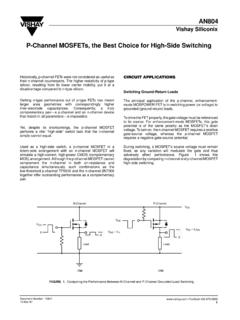
P-Channel MOSFETs, the Best Choice for High-Side Switching
www.vishay.comMOS) arrangement. Although the p-channel MOSFET cannot complement the n-channel in both on-resistance and capacitance simultaneously, such combinations as the low-threshold p-channel TP0610 and the n-channel 2N7000 together offer outstanding performance as a complementary pair. Switching Ground-Return Loads

Lecture 15: MOS Transistor models: Body effects, SPICE models
inst.eecs.berkeley.educircuits with FETs. zWe will also look at how SPICE models FETs for both small signal models and large signal models Department of EECS University of California, Berkeley EECS 105 Spring 2004, Lecture 15 Prof. J. S. Smith Small signal models: two terminals The current into a device depends on the history of voltages which have been applied to it
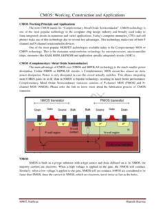
CMOS: Working, Construction and Applications
www.mpithathras.inCMOS (Complementary Metal Oxide Semiconductor) The main advantage of CMOS over NMOS and BIPOLAR technology is the much smaller power dissipation. Unlike NMOS or BIPOLAR circuits, a Complementary MOS circuit has almost no static ... There are two types of FETs: JFETs and MOSFETs. MOSFET is Metal Oxide Semiconductor Field Effect Transistor ...
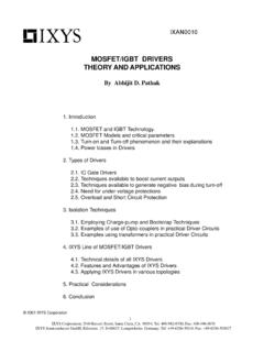
MOSFET/IGBT DRIVERS THEORY AND APPLICATIONS
www.ixys.comDue to the absence of minority carrier transport, MOS-FETs can be switched at much higher frequencies. The limit on this is imposed by two factors: transit time of elec-trons across the drift region and the time required to charge and discharge the input Gate and ‘Miller’ capacitances. IGBT derives its advantages from MOSFET and BJT. It
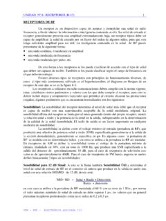
UNIDAD Nº 8 RECEPTORES (R-13) 1
www1.frm.utn.edu.arUNIDAD Nº 8– RECEPTORES (R-13) 2 UTN – FRM - ELECTRÓNICA APLICADA III Sensibilidad para 20 dB de aquietamiento: Esta indica el nivel de señal de RF de entrada que produce un silenciamiento o atenuación del ruido de salida del receptor de 20 dB, en este caso la

Les transistors et leurs applications - LAAS
homepages.laas.frcourant de fuite de la capacité MOS. Donc. la résistance. d’entrée. tend vers. l’infini. En règle générale, le substrat (bulk) est relié à la source Cette tension. V. T, est liée à la tension d’inversion de population dans le canal. Elle dépend des paramètres technologiques. Elle est très peu reproductible d’un transistor ...

BF998; BF998R Silicon N-channel dual-gate MOS-FETs
www.nxp.comSilicon N-channel dual-gate MOS-FETs BF998; BF998R LIMITING VALUES In accordance with the Absolute Maximum Rating System (IEC 134). Notes 1. Device mounted on a ceramic substrate, 8 mm 10 mm 0.7 mm. 2. Device mounted on a printed-circuit board. SYMBOL PARAMETER CONDITIONS MIN. MAX. UNIT VDS drain-source voltage 12 V ID drain current …