
Power Semiconductor Reliability Handbook
example, when the breakdown voltage needs to be changed, the simulation involves all the structure changes to optimize the breakdown voltage, threshold voltage, channel resistance, various parasitic capacitances, and the trade-off with UIS robustness, etc. For a new package design, thermal resistance is very important.
Download Power Semiconductor Reliability Handbook

Information
Domain:
Source:
Link to this page:
Documents from same domain

AOD4185/AOI4185 P-Channel Enhancement Mode …
www.aosmd.comParameter Symbol Maximum Units Absolute Maximum Ratings T C=25°C unless otherwise noted AOD4185/AOI4185 P-Channel Enhancement Mode Field Effect Transistor Features VDS (V) = -40V

High Voltage Power MOSFET switching …
www.aosmd.comHigh Voltage Power MOSFET switching parameters: Testing Methods for Guaranteeing datasheet limits Anup Bhalla, Fei Wang Introduction Power MOSFET datasheets will usually show typical and min-max values for Rg, Ciss, Crss, Coss, and also show values

Alpha and Omega Semiconductor Corporate …
www.aosmd.comAOS Corporate Responsibility 2 14064-1 worldwide standard, which means that we d evelop and implement programs to limit greenhouse gas (GHG) concentrations.

Continous Drain current rating and Bonding wire …
www.aosmd.comPower MOSFET Continuous Drain current rating and Bonding wire limitation Fei Wang , Kai Liu, Anup Bhalla Abstract Power MOSFET datasheets will usually show maximum values for continuous drain current Id, on the first page of

Power MOSFET Basics - Alpha and Omega …
www.aosmd.com1 Power MOSFET Basics Table of Contents 1. Basic Device Structure 2. Breakdown Voltage 3. On-State Characteristics 4. Capacitance 5. Gate Charge

100V N-Channel MOSFET
www.aosmd.comAOD478/AOI478 TYPICAL ELECTRICAL AND THERMAL CHARACTERISTICS 17 5 2 10 0 18 0 2 4 6 8 10 0 2 4 6 8 10 12 V GS (Volts) Qg …

Alpha & Omega Semiconductor
www.aosmd.com4 Summary of AOS Device / Process Qualification Monitor Results To present the actual FIT rate from the different process and device technologies, AOS

General Description Product Summary
www.aosmd.comAOD409/AOI409 TYPICAL ELECTRICAL AND THERMAL CHARACTERISTICS 0 2 4 6 8 10 0 10 20 30 40 50 60-V GS s) Q g (nC) Figure 7: Gate-Charge Characteristics 500

General Description Product Summary - Alpha and …
www.aosmd.comAO4294 General Description Product Summary VDS I D (at V GS =10V) 11.5A R DS(ON) (at V GS =10V) < 12mΩ R DS(ON) (at V GS =4.5V) < 15.5mΩ Applications 100% UIS Tested 100% Rg Tested Symbol

General Description Product Summary - Alpha and …
www.aosmd.comaonr21357 typical electrical and thermal characteristics 0 100 200 300) 400 500 1e-05 0.0001 0.001 0.01 0.1 1 10 100 pulse width (s)
Related documents
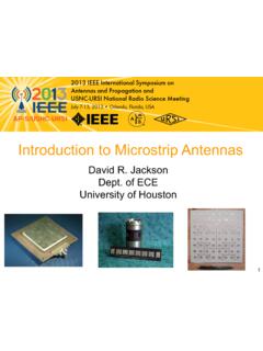
Introduction to Microstrip Antennas - University of Houston
courses.egr.uh.educonductor and dielectric losses*, and by surface-wave loss**. Only used at microwave frequencies and above (the substrate becomes too large at lower frequencies). Cannot handle extremely large amounts of power (dielectric breakdown). * Conductor and dielectric losses become more severe for thinner substrates.
Dielectric Materials: Properties and Applications
tiiciiitm.comThe dielectric materials can be classified into active and passive dielectric materials. i. Active dielectrics When a dielectric material is kept in an external electric field, if it actively accepts the electricity, then it is known as active dielectric material. Thus, active dielectrics are the dielectrics, which can easily adapt themselves

Testing Manual for Electrical Equipment - url
www.ppml.url.twDielectric Tests - It is presumed that every such equipment would also comply with the type test, since design is identical. The factory inspection and testing are conducted according to Company/international standards. The Inspection/testing of Electrical Equipment at Factory are carried out as per the flowchart attached below, 176

Dielectric Strength of Insulating Materials
chemistry.mdma.chgreater dielectric constant than that of the main liquid, the breakdown is the result of formation of ellipsoids from these dro ps by the electric field. In a strong enough electric field, these ellipsoids merge and form a high-conductivity channel between the electrodes.

HIGH VOLTAGE ENGINEERING(3:1:0), - Veer Surendra Sai ...
vssut.ac.inPost breakdown phenomena and applications, practical considerations in using gases for insulation purposes. MODULE-II (10 HOURS) Conduction and breakdown in liquid dielectrics: Pure liquids and commercial liquids, conduction and breakdown in pure liquids. Breakdown in solid dielectrics: Introduction, Intrinsic brakdown.