
SST25VF016B - Microchip Technology
Data Latches SuperFlash X - Decoder Memory Control Logic Address Buffers and Latches CE# Y - Decoder SCK SI SO WP# HOLD# Serial Interface. SST25VF016B DS20005044C-page 4 2015 Microchip Technology Inc. 2.0 PIN DESCRIPTION FIGURE 2-1: PIN ASSIGNMENTS ... SST25VF016B 1 2. 3-A 0 7 00. SST25VF016B 0)--). C 2 ...
Download SST25VF016B - Microchip Technology

Information
Domain:
Source:
Link to this page:
Documents from same domain

Power Factor Correction in Power Conversion …
ww1.microchip.com© 2007 Microchip Technology Inc. DS01106A-page 2 AN1106 FIGURE 1: CURRENT WAVEFORMS WITH AND WITHOUT PFC These waveforms illustrate that …

2.7V to 5.5V Single Supply CMOS Op Amp
ww1.microchip.comMCP601/1R/2/3/4 DS21314G-page 2 © 2007 Microchip Technology Inc. 1.0 ELECTRICAL CHARACTERISTICS Absolute Maximum Ratings † VDD –VSS.....7.0V

Data Encryption Routines for PIC24 and dsPIC Device
ww1.microchip.com© 2006 Microchip Technology Inc. DS01044A-page 1 AN1044 INTRODUCTION Currently, there are three data encryption standards approved …

Using SAM-BA for Linux on SAMA5D3 Xplained
ww1.microchip.comAN-8995 – Using SAM-BA for Linux on SAMA5D3 Xplained: 42328A−06/2014 Page 5 of 19 2. Setup With Ubuntu distributions, a user has to be member of the dialout group to access serial devices like

MCP6021/1R/2/3/4 - Rail-to-Rail Input/Output, 10 …
ww1.microchip.com2001-2017 Microchip Technology Inc. DS20001685E-page 1 MCP6021/1R/2/3/4 Features • Rail-to-Rail Input/Output • Wide Bandwidth: 10 MHz (typical)

Low Quiescent Current LDO - Microchip Technology
ww1.microchip.com2005-2016 Microchip Technology Inc. DS20001826D-page 1 MCP1700 Features: • 1.6 µA Typical Quiescent Current • Input Operating Voltage Range: 2.3V to 6.0V

MCP1703 250 mA, 16V, Low Quiescent Current
ww1.microchip.com2010 Microchip Technology Inc. DS22049E-page 1 MCP1703 Features: • 2.0 µA Typical Quiescent Current • Input Operating Voltage Range: 2.7V to16.0V

MTCH6102 Low-Power Projected Capacitive Touch …
ww1.microchip.com2014 Microchip Technology Inc. DS40001750A-page 1 Description: Microchip’s MTCH6102 is a turnkey projected capacitive touch controller that simplifies adding

PIC32 GUI Development Board with Projected …
ww1.microchip.comPIC32 GUI Development Board with Projected Capacitance (PCAP) Touch Information Sheet Microchip Technology Inc.

RN4020 Bluetooth Low Energy Module User’s Guide
ww1.microchip.comRN4020 BLUETOOTH LOW ENERGY MODULE USER’S GUIDE 2014 Microchip Technology Inc. DS70005191B-page 7 Preface INTRODUCTION This chapter contains general information that will be useful to know before using the
Related documents
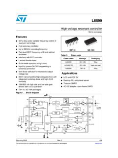
High-voltage resonant controller - STMicroelectronics
www.st.comA higher level OCP latches off the IC if the first- level protection is not su fficient to control the primary current. Their combination offers complete protection against overload and short circuits. An additional latched disable input (D IS) allows easy implementation of OTP and/or
Precision T3600 Owner's Manual
downloads.dell.comUnthread the cables from the latches. 5. Press on the clasp to release the latch holding the cables on the side of the optical-drive cage. 6. Press down on the latch and lift up the cables. 10. 7. Lift up the release latch on top of the ODD cage. 8. Holding the release latch, slide the optical-drive cage from the optical drive compartment.

Modeling Latches and Flip-flops - Xilinx
www.xilinx.comLatches Part 1 Storage elements can be classified into latches and flip-flops. A latch is a device with exactly two stable states: a high-output and a low-output. A latch has a feedback path, so information can be retained by the device. Therefore latches are volatile memory devices, and can store one bit of data for as long as the
Digital Phase Locked Loop - University of Maine
ece.umaine.eduThere are two D-latches used in PFD. Like any other regular D-latches they have a clock input, a data input, an inverted clear input and two opposite outputs, q and q bar. Each D-latch is made out of 4 three input nand gates and 2 two input nand gate. These nand gates are sized to give same delay as basic inverter.

Modeling Latches and Flip-flops - Xilinx
www.xilinx.comLatches Part 1 Storage elements can be classified into latches and flip-flops. Latch is a device with exactly two stable states: high-output and low-output. A latch has a feedback path, so information can be retained by the device. Therefore latches are volatile memory devices, and can store one bit of data for as long as the device is powered.

7. Latches and Flip-Flops - cs.ucr.edu
www.cs.ucr.eduChapter 7 – Latches and Flip-Flops Page 4 of 18 From the above analysis, we obtain the truth table in Figure 4(b) for the NAND implementation of the SR latch. Q is the current state or the current content of the latch and Qnext is the value to be updated in the next state. Figure 4(c) shows the logic symbol for the SR latch.