
The Bandgap Reference
resistor and a negative-TC resistor. Applying this idea to voltage quan-tities proved more difficult. It had been long recognized that the voltage across a forward-biased diode has a negative TC (if its bias current does not change much with temperature). However, a positive-TC voltage was missing. In 1964, Hilbiber of Fairchild
Download The Bandgap Reference

Information
Domain:
Source:
Link to this page:
Documents from same domain
Fundamentals of Chemical Reactor Theory1 - …
www.seas.ucla.edu1 UNIVERSITY OF CALIFORNIA, LOS ANGELES Civil & Environmental Engineering Department Fundamentals of Chemical Reactor Theory Michael K. Stenstrom
Introduction to Switched-Capacitor Circuits
www.seas.ucla.eduChapter 12. Introduction to Switched-Capacitor Circuits 398 Vout Vin C1 Vout V C C1 2 AB AB in0 (a) (b) Vin VA Vin0 t0 t Vin0 C1 C2 (c) Vout Figure 12.5. Circuit of Fig. 12.4 in (a) sampling mode, (b) amplification mode.

Noise in RF Design - Engineering
www.seas.ucla.eduEE215C B. Razavi Win. 13 HO #2 17 Example Noise Figure At high frequencies, it becomes difficult to measure the input-referred noise …
CMOS technology characterization for analog and …
www.seas.ucla.eduCMOS Technology Characterization for Analog and RF Design Behzad Razavi, Member, IEEE Abstract— The design of analog and radio-frequency (RF) circuits in CMOS technology becomes increasingly more difficult as device modeling faces new challenges in deep submicrometer processes and emerging circuit applications. The …

Analog Integrated Circuit Design - Engineering
www.seas.ucla.eduEE 215A HO#1 Fall 2014 Analog Integrated Circuit Design Instructor: Behzad Razavi 56-147D, Eng. IV
International Journal of Heat and Mass Transfer - …
www.seas.ucla.eduS;T refers to heat of mixing due to temperature gradient 638 A. d’Entremont, L. Pilon/International Journal of Heat and Mass Transfer 75 (2014) 637–649 depends on the ion concentration distribution and vice versa.

Seismic Code Requirements - Engineering
www.seas.ucla.eduBuilding Response Analysis zIn general, three types of analyses are done to design buildings subjected to earthquakes – Response History Analysis zLinear or nonlinear approach to calculate time varying responses (P, M, V, δ) – Response Spectrum Analysis zLinear approach to calculate modal responses (peak values) and combine modal responses
Physics of high-pressure helium and argon radio-frequency ...
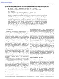
www.seas.ucla.eduThe physics of helium and argon rf discharges have been investigated in the pressure range from 50 to 760 Torr. The plasma source consists of metal electrodes that are perforated to allow the gas to
Fall 14 HO #8 - School of Engineering and Applied Science
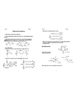
www.seas.ucla.eduEE215A B. Razavi Fall 14 HO #8 1 Differential Amplifiers Differential & Single-Ended Operation - A single-ended signal is taken with

L.Vandenberghe ECE133A(Fall2018) 5.Orthogonalmatrices
www.seas.ucla.eduProof thesquareddistanceofb toanarbitrarypointAx inrange„A”is kAx bk2 = kA„x xˆ”+ Axˆ bk2 (wherexˆ = ATb) = kA„x xˆ”k2 + kAxˆ bk2 +2„x xˆ”TAT„Axˆ b” = kA„x xˆ”k2 + kAxˆ bk2 = kx xˆk2 + kAxˆ bk2 kAxˆ bk2 withequalityonlyifx = xˆ line3followsbecauseAT„Axˆ b”= xˆ ATb = 0 line4followsfromATA = I Orthogonalmatrices 5.18
Related documents

Voltage Regulator Adjustment Guide
www.trtriumph.comnegative voltage is created. Since generators were created before semiconductors were readily available, there had to be a mechanical way to avoid making the wrong polarity voltage. ... voltage setting or in a counter clockwise direction to reduce the setting. Turn the screw only a fraction of the turn at a time and test after each adjustment ...

MAX1044/ICL7660 - Switched-Capacitor Voltage Converters
datasheets.maximintegrated.comNote 1: The Maxim ICL7660 and MAX1044 can operate without an external output diode over the full temperature and voltage ranges. The Maxim ICL7660 can also be used with an external output diode in series with pin 5 (cathode at VOUT) when
LT1964 Low Dropout Negative FEATURES - Analog Devices
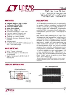
www.analog.comLow Dropout Negative Micropower Regulator The LT ®1964 is a micropower low noise, low dropout nega-tive regulator. The device is capable of supplying 200mA of output current with a dropout voltage of 340mV. Low quiescent current (30μA operating and 3μA shutdown) makes the LT1964 an excellent choice for battery-pow-ered applications ...
MT-087: Voltage References - Analog Devices
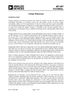
www.analog.comThe development of low voltage (<5 V) references based on the bandgap voltage of silicon led to the introductions of various ICs which could be operated on low voltage supplies with good TC performance. The first of these was the LM109 (Reference 1), and a basic bandgap reference cell is shown in Figure 2.
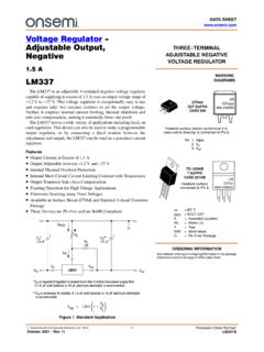
LM337 - Voltage Regulator - Adjustable Output, Negative
www.onsemi.comVoltage Regulator - Adjustable Output, Negative 1.5 A LM337 The LM337 is an adjustable 3−terminal negative voltage regulator capable of supplying in excess of 1.5 A over an output voltage range of −1.2 V to −37 V. This voltage regulator is exceptionally easy to use and requires only two external resistors to set the output voltage.

Negative Voltage Regulators - ON Semiconductor
www.onsemi.comNegative Voltage Regulators 100 mA MC79L00A Series The MC79L00A Series negative voltage regulators are inexpensive, easy−to−use devices suitable for numerous applications requiring up to 100 mA. Like the higher powered MC7900 Series negative regulators, this series features thermal shutdown and current limiting, making them remarkably rugged.

Mitigation technique of the SiC MOSFET gate voltage ...
www.st.comnegative voltage between -2 V and -5 V in according to the maximum rating of the involved device. The use of an active Miller clamp to mitigate induced G-S glitches allows to establish a low impedance path without compromising the turn-off slew rate control when the external switch is already off, which helps avoid the induced ...

LM137, LM337-N 3-Terminal Adjustable Negative Regulators ...
www.ti.comnegative voltage regulators capable of supplying • Line Regulation 0.01%/V (Typical) −1.5 A or more currents over an output voltage range • Load Regulation 0.3% (Typical) of −1.25 V to −37 V. It requires only two external • 77-dB Ripple Rejection resistors to …