
The Chip Scale Package (CSP) - Intel
lithography process reductions (die shrinks), so does the package. At a certain point, the associated ball pitch will get smaller as well, in order to accommodate the smaller size of the die. This eventually leads to ball pitches as small as .5mm and below. Currently the majority of µbga packages are in .75mm pitch.
Download The Chip Scale Package (CSP) - Intel

Information
Domain:
Source:
Link to this page:
Documents from same domain
Intel® AMT Configuration Utility User Guide
www.intel.comIntel® AMT Configuration Utility . User Guide . Version 11.0 . Document Release Date: December 17, 2015
Land Grid Array (LGA) Socket and Package …
www.intel.com3. Introduction. In this document, Intel has integrated customer feedback and developed a reference process to serve as a manufacturing enabling solution.
Microcode Revision Guide - intel.com
www.intel.comMicrocode Update Guidance Code Name Product Collection Product Names Vertical Segment CPUID Platform ID OS Update for Q2 Production Status Pre-Mitigation

U.S. Intern Relocation Guide (Including Canada)
www.intel.comFINDING HOUSING You are responsible for arranging your own housing needs, up to and including signing the lease, ordering rental furniture, paying deposits and setting up utilities.
DrMOS Specifications - Intel
www.intel.comTechnical Specifications R 7 3 Technical Specifications The feature set for the DrMOS can be divided into two major areas. They address the electrical
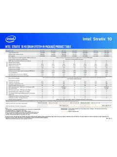
Intel Stratix 10
www.intel.comIntel® Stratix® 10 Intel ® StratIx® 10 Mx (DraM SySteM-In-Package) ProDuct table Notes: 1. LE counts valid in comparing across Intel FPGA devices, and …
Intel® Intel® Command Line InterfaceCommand …
www.intel.comIntel® Intel® Command Line InterfaceCommand Line InterfaceCommand Line Interface ... Intel® Command Line Interface Features and ... • Linux* command shell .
Data Sheet: MAX 3000A Programmable Logic …
www.intel.comAltera Corporation 3 MAX 3000A Programmable Logic Device Family Data Sheet The MAX 3000A architecture supports 100 % transistor-to-transistor logic
256 10 GX, MX, TX, and SX Device Family Pin …
www.intel.comIntel® Stratix® 10 GX Pin Connection Guidelines Clock and PLL Pins Note: Intel recommends that you create an Intel ® Quartus Prime design, enter your device I/O assignments, and compile the
256 10 L- and H-Tile Transceiver PHY User Guide - …
www.intel.comIntel® Stratix® 10 L- and H-Tile Transceiver PHY User Guide Subscribe Send Feedback UG-20055 | 2018.07.06 Latest document on the web: PDF | HTML
Related documents

Fabrication and Manufacturing (Basics)
people.ee.duke.edu– Photo-light lithography, n. process of printing from a plane surface on which image to be printed is ink-receptive and the blank area is ink-repellant • Cover the wafer with a light-sensitive, organic material called photoresist • Expose to light with the proper pattern (mask) • Patterns left by photoresist can be used to control where

Roll to Roll (R2R) Processing Technology Assessment
www.energy.gov172 Imprint or Soft Lithography – In soft lithography (e.g. self-aligned imprint lithography (SAIL)), 173 multiple mask levels are imprinted as a single three dimensional (3-D) structure as shown in 174 Figure 4. The photopolymer layer is heated above its glass transition temperature to allow it to 175 flow into the crevices of the stamp.
The Work of Art in the Age of Mechanical Reproduction
web.mit.eduLithography enabled graphic art to illustrate everyday life, and it began to keep pace with printing. But only a few decades after its invention, lithography was surpassed by photography. For the first time in the process of pictorial reproduction, photography freed the hand of the most important artistic
Introducing Intel Foundry Services
newsroom.intel.comMar 23, 2021 · drive the next generation of lithography innovation to deliver a new era of Moore's Law.” Peter Wennink, CEO and president, ASML “Cadence and Intel have forged a deep partnership to enable the design ecosystem to use Intel's leading-edge process technologies. With Intel's announcement today, we are excited to

Lithography Using ASML Stepper - diyhpl.us
diyhpl.usLithography Using ASML Stepper Page 4 INTRODUCTION Overlay (alignment) is as important as resolution in lithography. Modern CMOS integrated circuits have ~ 30 layers to be aligned. The RIT SUB-CMOS processes use up to 15 layers. Alignment marks are placed on the wafer at the beginning of the process

Optics for EUV Lithography
www.euvlitho.comOptics for EUV Lithography have evolved over three decades to a level where excellent imaging is demonstrated. Right now, the Starlith ® 3400 Optics extends EUV Lithography to 13nm single-shot resolution with high productivity for serial production. High-NA EUV Lithography enables further shrink for the

SPECIAL REPORTS 半導体リソグラフィ技術の動向と東芝の …
www.global.toshibaLithography technology, which transfers a device circuit pattern printed on a mask to a silicon wafer using an exposure tool, plays a critical role in the semiconductor device manufacturing process and is continuously evolving to realize the shrinkage of semiconductor devices. As optical