Transistor Technologies for High Efficiency and Linearity
Imax depends on device size Maximum power dissipation depends on size and duty cycle - worse for CW tone than for high PAR signals . Tradeoff of Breakdown Voltage and ft To avoid breakdown, generally must limit peak electric field to below ... HEMT pHEMT Si GaAs InP GaN .
Download Transistor Technologies for High Efficiency and Linearity

Information
Domain:
Source:
Link to this page:
Documents from same domain

Phase Locked Loop Circuits
web.ece.ucsb.eduClock generation: B. Razavi, Design of Analog CMOS Integrated Circuits, Chap. 15, McGraw-Hill, 2001. 1. Definition. A PLL is a feedback system that includes a VCO, phase detector, and low pass filter within its loop. Its purpose is to force the VCO to replicate and track the frequency and phase at the input when in lock.

ADS Tutorial Stability and Gain Circles ECE145A/218A
web.ece.ucsb.eduequations. The syntax is: gp_circle(S, gain, # points on circle) where S is the S-parameter matrix. Let’s illustrate. In the example below, a table is used to display frequency, maximum stable gain (MSG), the stability factor, k, and the magnitude of delta. The gain circles are at MSG (MaxGain1 in this case), and 1 and 2 dB below MSG.
Audio Amplifier Circuit - UC Santa Barbara
web.ece.ucsb.eduWeek #1: Audio amplifier Week #2: Microphone circuit The audio amplifier project is more difficult and time-consuming than the microphone pre-amp, so part of week #2 may be used to finish the audio amp. All breadboarding and testing can and should be done in lab. Soldering and hardwiring can and should be done outside lab.

Harmonic Balance Simulation on ADS
web.ece.ucsb.eduHarmonic Balance Simulation on ADS General Description of Harmonic Balance in Agilent ADS 1 Harmonic balance is a frequency-domain analysis technique for simulating nonlinear circuits and systems. It is well-suited for simulating analog RF and microwave circuits, ... function is driven to a given small value), then the resulting voltage ...
Quality factor, Q
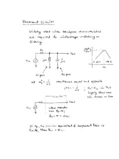
web.ece.ucsb.eduWhen a resonant circuit is connected to the outside world, its total losses (let’s call them RP or GP) are combined with the source and load resistances, RS and RL. For example, Here is a parallel resonant circuit (C,L and RP)connected to the outside. The total Q of this circuit is called the loaded Q or QL and is given by

Latches, the D Flip-Flop & Counter Design
web.ece.ucsb.eduFebruary 6, 2012 ECE 152A - Digital Design Principles 2 Reading Assignment Brown and Vranesic 7Flip-Flops, Registers, Counters and a Simple Processor 7.1 Basic Latch 7.2 Gated SR Latch 7.2.1 Gated SR Latch with NAND Gates 7.3 Gated D …

Flip-Flops and Sequential Circuit Design
web.ece.ucsb.edu11 Latches and Flip-Flops 11.5 S-R Flip-Flop 11.6 J-K Flip-Flop 11.7 T Flip-Flop 11.8 Flip-Flops with Additional Inputs 11.9 Summary 12 Registers and Counters 12.5 Counter Design Using S-R and J-K Flip-Flops 12.6 Derivation of Flip-Flop Input Equations – Summary

BASICS OF THE SPECTRUM ANALYZER - UC Santa Barbara
web.ece.ucsb.eduFourier ⋅ π → − + + Now instead of a bank of narrow filters, we shall have one narrow filter centered at a fixed frequency, say fI, and we shall scan the signal spectrum across this filter by multiplying x(t) by a sinusoid of varying frequency f0. See Figure 1. …

Mealy and Moore Machines
web.ece.ucsb.eduFebruary 22, 2012 ECE 152A - Digital Design Principles 5 Finite State Machines Two types (or models) of sequential circuits (or finite state machines) Mealy machine Output is function of present state and present input Moore machine Output is function of present state only Analysis first, then proceed to the design of
Number Representation and Computer Arithmetic
web.ece.ucsb.eduOne way to encode decimal digits using binary signals is to encode each of the digits 0-9 by means of its 4-bit binary representation. The resulting binary-coded decimal (BCD) representation is shown below:
Related documents

GaN Power HEMT Tutorial: GaN Basics
iganpower.comCommercial E-Mode GaN HEMT with “p-GaN” GIT: Gate with Ohmic Contact and Current Control Gate with Schottky Contact and Current Control 1,Kevin J. Chen, Understanding the Dynamic Behavior in GaN-on-Si Power Devices and IC’s, Integrated Power Conversion and Power Management, 2018

RF and Microwave Power Amplifier Design
nfs.gongkong.comdirectional couplers for RF and microwave power applications. So, for power combining in view of insufficient power performance of the ac-tive devices, it is best to use the coaxial cable combiners with ferrite core to combine the output powers of RF power amplifiers intended for wideband applications. As the device output impedance for high ...

Agilent ATF-54143 Low Noise Enhancement Mode …
www.ok2kkw.comTotal Power Dissipation[3] mW 360 P in max. RF Input Power dBm 10 T CH Channel Temperature °C 150 T STG Storage Temperature °C -65 to 150 θ jc Thermal Resistance[4] °C/W 162 Notes: 1. Operation of this device in excess of any one of these parameters may cause permanent damage. 2. Assumes DC quiescent conditions. 3. Source lead temperature ...
Status of the Power Electronics Industry - Flyer
s3.i-micronews.comdevice technology and reliability analysis (MOSFET, IGBT, HEMT, etc). In addition, Ana is leading the quarterly power management market updates released in 2017. Previously Ana was involved in a high-added value collaboration related to SJ Power MOSFETs, within the CNM research center for the leading power electronic company ON Semiconductor.

Status of Power Electronics Industry 2021
s3.i-micronews.comPOWER DEVICE POSITIONING AS A FUNCTION OF POWER AND FREQUENCY Power device technology positioning in 2021 103 102 101 100) Planar 103 Si Bipolar Operating frequency (Hz) 104 5 106 Si IGBT/IPM GaN Si Thyri stor SiC Si MOSFET GaN HEMT Competition zone Si/SiC/GaN Grid References to related Yole Développementand System …

Practical considerations when comparing SiC and GaN in ...
unitedsic.com60 milliohm device . This results in reduced gate-drive power and elimination of the danger of spurious turn-on due to drain positive-going dV/dt pushing spikes of current through the Miller capacitance into the gate-drive circuit. • There is energy lost in switching, E oss, associated with C oss. In the 650V

先端GaN-HEMTデバイス技術 - Fujitsu
www.fujitsu.commaterial properties also make the GaN-HEMT a good candidate for future power electronic devices, which must operate with a high drain current and high voltage. Fabricated normally-off GaN-HEMT devices showed a threshold voltage of 3 V, maximum drain current ... Fig.3-Characteristics for GaN MIS-HEMT device

NCP51820 - High Speed Half-Bridge Driver for GaN Power ...
www.onsemi.comDriver for GaN Power Switches NCP51820 The NCP51820 high−speed, gate driver is designed to meet the stringent requirements of driving enhancement mode (e−mode), high electron mobility transistor (HEMT) and gate injection transistor (GIT), gallium nitrade (GaN) power switches in off−line, half−bridge power topologies.