Transcription of 3URGXFW6SHFLILFDWLRQ 3( - psemi.com
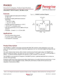
1 Page 1 of 13 Document No. DOC-81482-2 2017 Peregrine Semiconductor Corp. All rights reserved. Product Description The PE4312 is a 50 , HaRP technology-enhanced 6-bit RF Digital Step Attenuator (DSA) designed for use in 3G/4G wireless infrastructure and other high performance RF applications. This DSA is a pin-compatible upgraded version of the PE4302 with higher linearity, improved attenuation accuracy and faster switching speed. An integrated digital control interface supports both serial and parallel programming of the attenuation, including the capability to program an initial attenuation state at power-up. Covering a dB attenuation range in dB steps, it maintains high linearity and low power consumption from 1 MHz through 4 GHz. PE4312 also features an external negative supply option, and is offered in a 20-lead 4 4 mm QFN package. In addition, no external blocking capacitors are required if 0 VDC is present on the RF ports. The PE4312 is manufactured on Peregrine s UltraCMOS process, a patented variation of silicon-on-insulator (SOI) technology on a sapphire substrate.
2 Peregrine s HaRP technology enhancements deliver high linearity and excellent harmonics performance. It is an innovative feature of the UltraCMOS process, offering the performance of GaAs with the economy and integration of conventional CMOS. Product Specification UltraCMOS RF Digital Step Attenuator 6-bit, dB, 1 MHz 4 GHz Figure 1. Functional Schematic Diagram PE4312 Features Attenuation: dB steps to dB Safe attenuation state transitions Monotonicity: dB up to 4 GHz High attenuation accuracy ( + 1% x Atten) @ 1 GHz ( + 2% x Atten) @ GHz ( + 8% x Atten) @ 4 GHz High linearity: +59 dBm IIP3 Wide power supply range of control logic compatible 105 C operating temperature Programming modes Direct parallel Latched parallel Serial Unique power-up state selection Pin compatible to PE4302, PE4305 and PE4306 Control Logic InterfaceParallel ControlPower-Up ControlSerial ControlRF InputRF OutputSwitched Attenuator Array632 Figure 2. Package Type 20-lead 4 4 mm QFN DOC-02132 Product Specification PE4312 Page 2 of 13 2017 Peregrine Semiconductor Corp.
3 All rights reserved. Document No. DOC-81482-2 UltraCMOS RFIC Solutions Table 1. Electrical Specifications @ 25 C (ZS= ZL = 50 ), unless otherwise noted Normal Mode1: VDD = , VSS_EXT = 0V or Bypass Mode2: VDD = , VSS_EXT = Parameter Condition Min Typ Max Unit Frequency Operation frequency 1 4000 MHz Attenuation range dB step 0 dB Insertion loss dB dB dB 1 MHz <1 GHz 1 GHz 4 GHz Attenuation error Any bit or bit combination ( + 1% of atten setting) ( + 2% of atten setting) ( + 8% of atten setting) dB dB dB 1 MHz 1 GHz 1 < GHz 4 GHz Return loss (input or output port) 14 10 18 17 dB 1 GHz 4 GHz Input compression point3 30 dBm 1 MHz 4 GHz Input IP3 Two tones at +18 dBm, 10 kHz spacing 59 dBm 1950 MHz Switching time 50% CTRL to 90% or 10% RF 500 800 ns Notes: 1. Normal mode: single external positive supply used. 2. Bypass mode: both external positive supply and external negative supply used. 3. The input compression point is a linearity figure of merit.
4 Refer to Table 5 for the operating RF input power (50 ). Product Specification PE4312 Page 3 of 13 Document No. DOC-81482-2 2017 Peregrine Semiconductor Corp. All rights reserved. VDDPUP1 PUP2 VDDGND1201918171615141312116789102345C16 RF1 DataClockLEGNDVSS_EXT/ Ground PadTable 2. Pin Descriptions Figure 3. Pin Configuration (Top View) Pin # Pin Name Description 1 C163,5 Attenuation control bit, 16 dB 2 RF11 RF1 port (RF input) 3 Data3 Serial interface data input 4 Clock Serial interface clock input 5 LE4 Latch Enable input 6 VDD Supply voltage (nominal ) 7 PUP15 Power-up selection bit 1 8 PUP2 Power-up selection bit 2 9 VDD Supply voltage (nominal ) 10, 11, 18 GND Ground 12 VSS_EXT/GND2 External VSS negative voltage control or ground 13 P/S Parallel/Serial mode select 14 RF21 RF2 port (RF output) 15 C8 Attenuation control bit, 8 dB 16 C4 Attenuation control bit, 4 dB 17 C2 Attenuation control bit, 2 dB 19 C1 Attenuation control bit, 1 dB 20 Attenuation control bit, dB Pad GND Exposed pad: ground for proper operation Table 4.
5 Absolute Maximum Ratings Table 3. Operating Ranges Parameter Symbol Min Max Unit Supply voltage VDD V Digital input voltage VCTRL V Maximum input power PMAX_ABS +30 dBm Storage temperature range TST -65 +150 C ESD voltage HBM*, all pins VESD 1500 V Parameter Symbol Min Typ Max Unit Normal mode1 Supply voltage VDD V Supply current IDD 130 200 A Bypass mode2 Supply voltage VDD V Supply current IDD 50 80 A Negative supply voltage VSS_EXT V Negative supply current ISS -40 -16 A Normal or Bypass mode Digital input high V Digital input low V Digital input leakage3 20 A RF input power, CW 1 50 MHz >50 MHz 4 GHz PMAX_CW Fig. 4 +24 dBm dBm RF input power, pulsed4 1 50 MHz >50 MHz 4 GHz PMAX_PULSED Fig. 4 +27 dBm dBm Operating temperature range TOP -55 +105 C Exceeding absolute maximum ratings may cause permanent damage. Operation should be restricted to the limits in the Operating Ranges table. Operation between operating range maximum and absolute maximum for extended periods may reduce reliability.
6 Note: * Human Body Model (MIL-STD-883 Method 3015) Notes: 1. Normal mode: connect pin 12 to GND to enable internal negative voltage generator. 2. Bypass mode: apply a negative voltage to VSS_EXT (pin 12) to bypass and disable internal negative voltage generator. 3. Applies to all pins except pins 1, 5, 7 and 20. Pins 1, 7 and 20 have an internal pull-down resistor and pin 5 has an internal pull-up resistor. 4. Pulsed, 5% duty cycle of 4620 s period, 50 . Pin 1 dot marking Notes: 1. RF pins 2 and 14 must be at 0 VDC. The RF pins do not require DC blocking capacitors for proper operation if the 0 VDC requirement is met. 2. Use VSS_EXT (pin 12, refer to Table 3) to bypass and disable internal negative voltage generator. Connect VSS_EXT (pin 12, VSS_EXT = GND) to enable internal negative voltage generator. 3. Place a 10 k resistor in series, as close to pin as possible to avoid frequency resonance. 4. This pin has an internal 2 M resistor to internal positive digital supply. 5.
7 This pin has an internal 200 k resistor to GND. Product Specification PE4312 Page 4 of 13 2017 Peregrine Semiconductor Corp. All rights reserved. Document No. DOC-81482-2 UltraCMOS RFIC Solutions Electrostatic Discharge (ESD) Precautions When handling this UltraCMOS device, observe the same precautions that you would use with other ESD-sensitive devices. Although this device contains circuitry to protect it from damage due to ESD, precautions should be taken to avoid exceeding the rate specified. Latch-Up Avoidance Unlike conventional CMOS devices, UltraCMOS devices are immune to latch-up. Switching Frequency The PE4312 has a maximum 25 kHz switching rate in normal mode (pin 12 = GND). A faster switching rate is available in bypass mode (pin 12 = VSS_EXT). The rate at which the PE4312 can be switched is then limited to the switching time as specified in Table 1. Switching frequency describes the time duration between switching events. Switching time is the time duration between the point the control signal reaches 50% of the final value and the point the output signal reaches within 10% or 90% of its target value.
8 Resistor on Pin 1 & 3 A 10 k resistor on the inputs to pin 1 and 3 (see Figure 26) will eliminate package resonance between the RF input pin and the two digital inputs. Specified attenuation error versus frequency performance is dependent upon this condition. Moisture Sensitivity Level The moisture sensitivity level rating for the PE4312 in the 4 4 mm QFN package is MSL1. Spurious Performance The typical low-frequency spurious performance of the PE4312 in normal mode is 140 dBm (pin 12 = GND). If spur-free performance is desired, the internal negative voltage generator can be disabled by applying a negative voltage to VSS_EXT (pin 12). Safe Attenuation State Transitions The PE4312 features a novel architecture to provide safe transition behavior when changing attenuation states. When RF input power is applied, positive output power spikes are prevented during attenuation state changes by optimized internal timing control. Figure 4. Power Derating Curve for 1 50 MHz 0246810121416182022242628300510152025303 5404550 Input Power (dBm)Frequency (MHz)RF Input Power, CW or Pulsed (-40C to 105C)Product Specification PE4312 Page 5 of 13 Document No.
9 DOC-81482-2 2017 Peregrine Semiconductor Corp. All rights reserved. Programming Options Parallel/Serial Selection Either a parallel or serial interface can be used to control the PE4312. The P/S bit provides this selection, with P/S = LOW selecting the parallel interface and P/S = HIGH selecting the serial interface. Parallel Mode Interface The parallel interface consists of six CMOS-compatible control lines that select the desired attenuation state, as shown in Table 5. The parallel interface timing requirements are defined by Figure 5 (Parallel Interface Timing Diagram), Table 9 (Parallel Interface AC Characteristics), and switching speed (Table 1). For latched parallel programming the Latch Enable (LE) should be held LOW while changing attenuation state control values, then pulse LE HIGH to LOW (per Figure 5) to latch the new attenuation state into the device. For direct parallel programming, the Latch Enable (LE) line should be pulled HIGH. Changing attenuation state control values will change device state to new attenuation.
10 Direct Mode is ideal for manual control of the device (using hardwire, switches, or jumpers). P/S C16 C8 C4 C2 C1 Attenuation State 0 0 0 0 0 0 0 Reference Loss 0 0 0 0 0 0 1 dB 0 0 0 0 0 1 0 1 dB 0 0 0 0 1 0 0 2 dB 0 0 0 1 0 0 0 4 dB 0 0 1 0 0 0 0 8 dB 0 1 0 0 0 0 0 16 dB 0 1 1 1 1 1 1 dB Table 5. Truth Table* Note: * Not all 64 possible combinations of C16 are shown in table. Serial Interface The serial interface is a 6-bit serial-in, parallel-out shift register buffered by a transparent latch. It is controlled by three CMOS-compatible signals: Data, Clock, and Latch Enable (LE). The Data and Clock inputs allow data to be serially entered into the shift register, a process that is independent of the state of the LE input. The LE input controls the latch. When LE is HIGH, the latch is transparent and the contents of the serial shift register control the attenuator. When LE is brought LOW, data in the shift register is latched. The shift register should be loaded while LE is held LOW to prevent the attenuator value from changing as data is entered.