Transcription of AO4441 Rev.2.0 Rohs - Alpha & Omega …
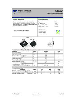
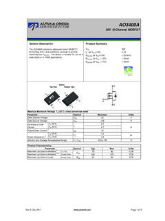
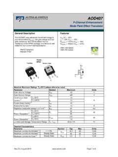
1 AO444160V P-Channel MOSFETG eneral DescriptionProduct SummaryVDS ID (at VGS=-10V)-4A RDS(ON) (at VGS=-10V)< 100m RDS(ON) (at VGS = )< 130m SymbolVDSThe AO4441 uses advanced trench technology to provideexcellent RDS(ON), and ultra-low low gate charge. Thisdevice is suitable for use as a load switch or in Maximum Ratings TA=25 C unless otherwise noted-60 VDrain-Source Voltage-60 GDSSOIC-8 Top View Bottom View DDDDSSSGVGSIDMTJ, TSTGS ymbolt 10sSteady-StateSteady-StateR JLMaximum Junction-to-Lead C C/W C/WMaximum Junction-to-Ambient A217530TA=25 CTA=70 CPower Dissipation APDP ulsed Drain Current BContinuous DrainCurrent ATA=25 20 Gate-Source VoltageUnitsParameterTypMax C/WR JA245440 Maximum Junction-to-Ambient AThermal CJunction and Storage Temperature Range-55 to 150 C.
2 August 1 of 5 AO4441 SymbolMinTypMaxUnitsBVDSS-60 VVDS=-48V, VGS=0V-1TJ=55 C-5 IGSS 100nAVGS(th)Gate Threshold C130102130m Qg(10V)1620nCQg( ) (on) Characteristics (TJ=25 C unless otherwise noted)STATIC PARAMETERSP arameterConditionsDrain-Source Breakdown VoltageID=-250 A, VGS=0 VVGS=-10V, ID=-4 ARDS(ON)Static Drain-Source On-ResistanceIDSS AVDS=VGS, ID=-250 AVDS=0V, VGS= 20 VZero Gate Voltage Drain CurrentGate-Body leakage currentm IS=-1A,VGS=0 VVDS=-5V, ID=-4 AVGS= , ID=-3 AForward TransconductanceDiode Forward VoltageTurn-On Rise TimeTurn-Off DelayTimeMaximum Body-Diode Continuous CurrentInput CapacitanceOutput CapacitanceTurn-On DelayTimeDYNAMIC PARAMETERSVGS=-10V, VDS=-30V, RL= ,R=3 Reverse Transfer CapacitanceVGS=0V, VDS=-30V, f=1 MHzSWITCHING PARAMETERSGate resistancef=1 MHzTotal Gate ChargeVGS=-10V, VDS=-30V.
3 ID=-4 AGate Source ChargeGate Drain ChargeTotal Gate ChargetD(off) PRODUCT HAS BEEN DESIGNED AND QUALIFIED FOR THE CONSUMER MARKET. APPLICATIONS OR USES AS CRITICAL COMPONENTS IN LIFE SUPPORT DEVICES OR SYSTEMS ARE NOT AUTHORIZED. AOS DOES NOT ASSUME ANY LIABILITY ARISINGOUT OF SUCH APPLICATIONS OR USES OF ITS PRODUCTS. AOS RESERVES THE RIGHT TO IMPROVE PRODUCT DESIGN,FUNCTIONS AND RELIABILITY WITHOUT Diode Reverse Recovery TimeBody Diode Reverse Recovery ChargeIF=-4A, dI/dt=100A/ sTurn-Off DelayTimeIF=-4A, dI/dt=100A/ sTurn-Off Fall TimeRGEN=3 A: The value of R JAis measured with the device mounted on 1in2FR-4 board with 2oz.
4 Copper, in a still air environment with TA =25 C. The value in any a given application depends on the user's specific board design. The current rating is based on the t 10s thermal resistance : Repetitive rating, pulse width limited by junction The R JAis the sum of the thermal impedence from junction to lead R JLand lead to The static characteristics in Figures 1 to 6,12,14 are obtained using 80 s pulses, duty cycle These tests are performed with the device mounted on 1 in2FR-4 board with 2oz. Copper, in a still air environment with TA=25 C. The SOA curve provides a single pulse rating.
5 : August 2 of 5 AO4441 TYPICAL ELECTRICAL AND THERMAL CHARACTERISTICS02468100123456-ID(A)-VGS( Volts)Figure 2: Transfer Characteristics7080901001100246810 RDS(ON)(m )-ID(A)Figure 3: On-Resistance vs. Drain Current and Gate On-ResistanceTemperature ( C)Figure 4: On-Resistance vs. Junction TemperatureVGS= C125 CVDS=-5 VVGS= (A)-VDS(Volts)Fig 1: On-Region CharacteristicsVGS= + + (A)-VSD(Volts)Figure 6: Body-Diode Characteristics25 C125 C6080100120140160180200246810 RDS(ON)(m )-VGS(Volts)Figure 5: On-Resistance vs. Gate-Source VoltageID=-4A25 C125 C : August 3 of 5 AO4441 TYPICAL ELECTRICAL AND THERMAL (Amps)-VDS(Volts)-VGS> or equal to 9: Maximum Forward Biased Safe Operating Area (Note E)10 s1s1msDCRDS(ON) limitedTJ(Max)=150 CTA=25 C100 (Volts)Qg(nC)Figure 7: Gate-Charge Characteristics0300600900120015000510152 025 Capacitance (pF)-VDS(Volts)Figure 8: Capacitance CharacteristicsCissCossCrssVDS=-30 VID= (W)Pulse Width (s)Figure 10.
6 Single Pulse Power Rating Junction-to-Ambient (Note E)10msTJ(Max)=150 CTA=25 JANormalized Transient Thermal ResistancePulse Width (s)Figure 11: Normalized Maximum Transient Thermal ImpedanceD=Ton/TTJ,PK=TA+ JAR JA=75 C/WIn descending orderD= , , , , , , single pulse : August 4 of 5 AO4441 VDCIgVdsDUTVDCVgsVgsQgQgsQgdChargeGate Charge Test Circuit & Waveform-+-+-10 VVddIdVgsVdsUnclamped Inductive Switching (UIS) Test Circuit & WaveformsVdsL-2E = 1/2 LIARARBVDSSVDCDUTVddVgsVdsVgsRLRgResisti ve Switching Test Circuit & Waveforms-+VgsVdstttttt90%10%rond(off)fo ffd(on)VddVgsVgsRgDUTVDCVgsIdVgs-+IARIgV gs-+VDCDUTLVgsIsdDiode Recovery Test Circuit & W aveformsVds -Vds +dI/dtRMrrVddVddQ = - Idttrr-Isd-VdsF-I-I : August 5 of 5