Transcription of AP7333 - Diodes Incorporated
1 AP7333 . 300mA, Low Quiescent Current, fast transient Low Dropout Linear Regulator Features Description 300mA Low Dropout Regulator in 3-pin package The AP7333 is a 300mA, fixed output voltage, low dropout linear Very low IQ over full load: 65 A regulator. The device included pass element, error amplifier, band-gap, current limit and thermal shutdown circuitry. Wide input voltage range: 2V to 6V. Fixed output options: to The characteristics of low dropout voltage and low quiescent PSRR: 65dB typical at 100Hz current make it suitable for low power applications, for example, fast start-up time: 80 s battery powered devices. The typical quiescent current is approximately 65 A. Stable with low ESR, 1 F ceramic output capacitor Excellent Load/Line transient Response Built-in current-limit and thermal-shutdown functions prevent IC. Low dropout: 300mV typical at 300mA from damage in fault conditions. Current limit protection Short circuit protection The AP7333 is available in SOT23 packages with different pin-outs.
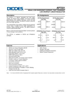
2 Thermal shutdown protection Ambient temperature range: -40 C to 85 C. SOT23 and SOT23R: Available in Green Molding Compound (No Br, Sb). Lead Free Finish/RoHS Compliant (Note 1). Applications XDSL Router Wireless LAN Cards Desktop and Notebook Computers Battery Powered Equipments Mouse, Keyboards Typical Application Circuit VIN VOUT. IN OUT. AP7333 . 1uF 1uF. GND. AP7333 Rev. 2 1 of 12 NOVEMBER 2009. Diodes Incorporated AP7333 . 300mA, Low Quiescent Current, fast transient Low Dropout Linear Regulator Ordering Information AP7333 - XX XX G - 7. Output Package Green Packing 10 : SA : SOT23 G : Green 7 : Tape & Reel 12 : SR : SOT23R. 15 : 18 : 20 : 25 : 28 : 30 : 33 : Packaging 7 Tape and Reel Device Package Code (Note 2) Quantity Part Number Suffix AP7333 -XXSAG-7 SA SOT23 3000/Tape & Reel -7. AP7333 -XXSRG-7 SR SOT23R 3000/Tape & Reel -7. Notes: 1. EU Directive 2002/95/EC (RoHS). All applicable RoHS exemptions applied. Please visit our website at 2. Pad layout as shown on Diodes Inc. suggested pad layout document AP02001, which can be found on our website at Pin Assignment (1) SOT23 (1) SOT23R.
3 ( Top View ) ( Top View ). IN 1 GND 1. 3 GND 3 IN. OUT 2 OUT 2. AP7333 Rev. 2 2 of 12 NOVEMBER 2009. Diodes Incorporated AP7333 . 300mA, Low Quiescent Current, fast transient Low Dropout Linear Regulator Pin Descriptions Pin Number Pin Name Description SOT23 SOT23R. Voltage input pin. Bypass to ground through at least 1 F. IN 1 3. capacitor Voltage output pin. Bypass to ground through 1 F ceramic OUT 2 2. capacitor GND 3 1 Ground Functional Block Diagram IN OUT. C urre nt Lim it G ate and T herm a l D river S hutdow n R. V REF. R. GND. AP7333 Rev. 2 3 of 12 NOVEMBER 2009. Diodes Incorporated AP7333 . 300mA, Low Quiescent Current, fast transient Low Dropout Linear Regulator Absolute Maximum Ratings Symbol Parameter Ratings Units ESD HBM Human Body Model ESD Protection 6 kV. ESD MM Machine Model ESD Protection 400 V. VIN Input Voltage 7 V. Continuous Load Current Internal Limited TOP Operating Junction Temperature Range -40 ~ 125 C. TST Storage Temperature Range -65 ~150 C. SOT23 600 mW.
4 PD Power Dissipation (Note 3). SOT23R 540 mW. TJ Maximum Junction Temperature 150 C. Recommended Operating Conditions Symbol Parameter Min Max Unit VIN Input voltage 2 6 V. IOUT Output Current (Note 4) 0 300 mA. TA Operating Ambient Temperature -40 85 C. Notes: 3. Ratings apply to ambient temperature at 25 C. 4. The device maintains a stable, regulated output voltage without a load current. AP7333 Rev. 2 4 of 12 NOVEMBER 2009. Diodes Incorporated AP7333 . 300mA, Low Quiescent Current, fast transient Low Dropout Linear Regulator Electrical Characteristics o (TA = 25 C, VIN = VOUT +1V, CIN = 1uF, COUT = 1uF, unless otherwise stated). Symbol Parameter Test Conditions Min Typ. Max Unit IOUT = 0mA 55 75. IQ Input Quiescent Current A. IOUT = 300mA 65 85. VDropout Dropout Voltage (Note 5) IOUT = 300mA 300 550 mV. TA = -40oC to 85oC, VOUT Output Voltage Accuracy -2 2 %. IOUT = 30mA. VOUT VIN = (VOUT +1V) to VIN-Max, Line Regulation %/V. / VIN/V IOUT = 1mA. VOUT VIN = (VOUT +1V) to VIN-Max, Load Regulation %.
5 /VOUT IOUT from 1mA to 300mA. VIN = 0V to , VOUT = 1V, tST Start-up Time 80 s IOUT = 300mA. VIN = [VOUT +1V]VDC + , PSRR PSRR 65 dB. f = 100Hz, IOUT = 30mA. VIN = VIN-Min to VIN-Max, ISHORT Short-circuit Current 100 mA. VOUT < ILIMIT Current Limit VOUT/ROUT = 1A 400 600 mA. TSHDN Thermal Shutdown Threshold 140 C. THYS Thermal Shutdown Hysteresis 15 C. o SOT23 (Note 6) 207 C/W. JA Thermal Resistance Junction-to-Ambient o SOT23R (Note 6) 230 C/W. Notes: 5. Dropout voltage is the voltage difference between the input and the output at which the output voltage drops 2% below its nominal value. This parameter only applies to output voltages above 6. Test conditions for SOT23 and SOT23R: Device mounted on FR-4 substrate PCB, with minimum recommended pad layout, 2oz copper, single sided. AP7333 Rev. 2 5 of 12 NOVEMBER 2009. Diodes Incorporated AP7333 . 300mA, Low Quiescent Current, fast transient Low Dropout Linear Regulator Typical Performance Characteristics Quiescent Current vs Input Voltage Line Regulation (% /V).
6 Iload=0mA. 60. Output Voltage Variation (%/V). Vout= 90 . 58 90 . Output Current (mA). 56. 54. 52. 25 -45 Vout= 25 -45 . 50. Vin=Vout +1V. 48 3 6 4 5 6. Input Voltage (V) Input Voltage (V). Load Regulation (% ) Dropout Voltage 350. Vout= 90 . -45 300. Output Voltage Variation (%). Dropout Voltage (mV). 250. 200. 0. 150. 100 25 -45 . 25 . Vout= 50. Vin=Vout +1V 90 . 0. 0 50 100 150 200 250 300. 0 50 100 150 200 250 300. Output Current (mA) Output Current (mA). Short Circuit vs Input Voltage Current Limit vs Input Voltage 105 600. Vout= Ta=25 . 100 -45 . Vout= Current Limit (mA). Output Current (mA). 550. 95. 90 500. 85. 450. 80. 25 90 . 400. 75. 4 5 6 4 5 6. Input Voltage (V). Input Voltage (V). AP7333 Rev. 2 6 of 12 NOVEMBER 2009. Diodes Incorporated AP7333 . 300mA, Low Quiescent Current, fast transient Low Dropout Linear Regulator Typical Performance Characteristics (Continued). PSRR PSRR. 75 75. 70 70. Vout=1V Vout= 65 Vin=2V 65 Vin= Cin=Cout=1uF Cin=Cout=1uF. 60 Ta=25 60 Ta=25.
7 PSRR (dB). PSRR (dB). 55 55. 50 50. 45 45. 40 40. 35 35. 1 10 100 1 10 100. Frequency (kHz) Frequency (kHz). Line transient Response Line transient Response Vin=3V to 2V (1V/div). Vin=2V to 3V (1V/div) Tr=10us Tr=10us Vout=1V (50mV/div) Vout=1V (50mV/div). Iout=300mA (300mA/div) Iout=300mA (300mA/div). Time (50us/div) Time (50us/div). AP7333 Rev. 2 7 of 12 NOVEMBER 2009. Diodes Incorporated AP7333 . 300mA, Low Quiescent Current, fast transient Low Dropout Linear Regulator Typical Performance Characteristics (Continued). Load transient Response Load transient Response Tr=Tf=10us Tr=Tf=10us Vin=2V Vin= Vout=1V Vout= (100mV/div) (100mV/div). Iout=1mA to 300mA Iout=1mA to 300mA. (100mA/div) (100mA/div). Time (200us/div) Time (200us/div). Start-Up Time (No Load) Start-Up Time (300mA Load). Vin=0 to (1V/div) Vin=0 to (1V/div). Cin=Cout=1uF Cin=Cout=1uF. Vout= (1V/div) Vout= (1V/div). Iout (300mA/div). Time (50us/div) Time (50us/div). AP7333 Rev. 2 8 of 12 NOVEMBER 2009. Diodes Incorporated AP7333 .
8 300mA, Low Quiescent Current, fast transient Low Dropout Linear Regulator Application Note Input Capacitor to cool down. When the junction temperature reduces to approximately +125 C the output circuitry is enabled again. A 1 F ceramic capacitor is recommended to connect between Depending on power dissipation, thermal resistance, and VIN and GND pins to decouple input power supply glitch and ambient temperature, the thermal protection circuit may cycle noise. The amount of the capacitance may be increased on and off. This cycling limits the heat dissipation of the without limit. This input capacitor must be located as close as regulator, protecting it from damage due to overheating. possible to the device to assure input stability and less noise. For PCB layout, a wide copper trace is required for both VIN and Ultra fast Start-up GND. A lower ESR capacitor allows the use of less After turned on, the AP7333 is able to provide full power in as capacitance, while higher ESR type requires more little as tens of microseconds, typically 80 s, without sacrificing capacitance.
9 Low ground current. This feature will help load circuitry move in and out of standby mode in real time, eventually extend battery Output Capacitor life for mobile phones and other portable devices. The output capacitor is required to stabilize and help transient response for LDO. The AP7333 is stable with very small fast transient Response ceramic output capacitors. The recommended capacitance is fast transient response LDOs can also extend battery life. from 1 F to F, Equivalent Series Resistance (ESR) is from TDMA-based cell phone protocols such as Global System for 10m to 200m , and temperature characteristic is X7R or X5R. Mobile Communications (GSM) have a transmit/receive duty Higher capacitance values help to improve load/line transient factor of only percent, enabling power savings by putting response. The output capacitance may be increased to keep much of the baseband circuitry into standby mode in between low undershoot/overshoot. Place output capacitor as close as transmit cycles.
10 In baseband circuits, the load often transitions possible to OUT and GND pins, and keep the leads as short as virtually instantaneously from 100 A to 100mA. To meet this possible. load requirement, the LDO must react very quickly without a large voltage drop or overshoot a requirement that cannot be met with conventional, general-purpose LDOs. No Load Stability No minimum load is required to keep the device stable. The The AP7333 's fast transient response from 0 to 300mA. device will remain stable and regulated in no load condition. provides stable voltage supply for fast DSP and GSM chipset with fast changing load. Current Limit Protection When output current at OUT pin is higher than current limit Small Overshoot and Undershoot threshold, the current limit protection will be triggered and The AP7333 has small and controlled overshoot and clamp the output current to approximately 600mA to prevent undershoot in load and line transitions. This helps to protect over-current and to protect the regulator from damage due to supplied circuit from damage and operation error caused by overheating.