Search results with tag "Differential input"

MT-041: Op Amp Input and Output Common ... - Analog …
www.analog.comCertain input structures require limiting of differential input voltage to prevent damage. These op amps will generally have internal back-to-back diodes across the inputs. This will not always show up in the simplified schematics of the amps. It will show up, however, as a differential input voltage specification of ±700 mV maximum.

A Differential Op-Amp Circuit Collection - uni-lj.si
www.fmf.uni-lj.sidifferential logic have been exploited for 2 decades. More recently, advanced high-speed A/D converters have adopted differential inputs. Single-ended op-amps require a problematic transformer to interface to these differential input A/D converters. This is the application that spurred the development of fully-differential op-amps.

PCA82C250 CAN controller interface - NXP
www.nxp.comRi input resistance CANH, CANL 5 - 25 k Rdiff differential input resistance 20 - 100 k Ci input capacitance CANH, CANL - - 20 pF Cdiff differential input capacitance - - 10 pF Reference output Vref reference output voltage V8 =1V; 50 A<I5 <50 A 0.45VCC - 0.55VCC V V8 =4V; 5 A<I5 <5 A0.4VCC-0.6VCC V

AD8131 Low Cost, High Speed Differential ... - Analog Devices
www.analog.comThe AD8131 is a differential or single-ended input to differential output driver requiring no external components for a fixed gain of 2. The AD8131 is a major advancement over op amps for driving signals over long lines or for driving differential input ADCs. The AD8131 has …

DECEMBER 2009 High-Speed,Fully Differential, Programmable ...
www.ti.comPGA870 www.ti.com SBOS436A –DECEMBER 2009–REVISED FEBRUARY 2011 ELECTRICAL CHARACTERISTICS: VS+= +5 V Boldface limits are tested at +25°C. At TA= +25°C, VS+= +5 V, differential input signal, differential VOUT = 2 VPP, RL= 200 Ωdifferential, G = 20 dB, and input and output common-modeat internal midsupply reference, unless otherwise noted.
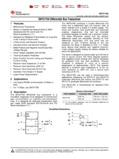
SN75176A Differential Bus Transceiver - Texas Instruments
www.ti.comThe SN75176A combines a 3-state differential line driver and a differential input line receiver, both of which operate from a single 5-V power supply. The driver and receiver have active-high and active-low enables, respectively, that can be externally connected together to function as a direction control. The driver differential outputs and ...

LM111, LM211, LM311 Differential Comparators datasheet ...
www.ti.comVID Differential input voltage(3) ±30 V VI Input voltage (either input)(2)(4) ±15 V Voltage from emitter output to VCC– 30 V Voltage from collector output to VCC– LM111 50 V LM211 50 LM211Q 50 LM311 40 Duration of output short circuit to ground 10 s TJ Operating virtual-junction temperature 150 °C Case temperature for 60 s FK package 260 °C
LF353-NWide Bandwidth Dual JFET Input Operational Amplifier
www.ti.comThe maximum differential input voltage is independent of the supply voltages. However, neither of the input voltages should be allowed to exceed the negative supply as this will cause large currents to flow which can result in a destroyed unit. Exceeding the negative common-mode limit on either input will force the output to a high state ...

Data Sheet NAU780x - Nuvoton
www.nuvoton.comAug 31, 2010 · ANALOG INPUT Full-scale input range (VINxP – VINxN) ± 0.5/(VREF/PGA) VREF = REFP V REFN Common mode range with PGA gain 64, 128 AVSS + 1.5 AVDD – 1.5 V Common mode range with PGA bypass enabled AVSS - 0.1 AVDD + 0.1 V Differential input impedance 5 GΩ PGA bypass=off, DC Bandwidth (-3dB) 2.27 Hz Data output rate = 10 SPS

PAC1931/PAC1932/PAC1933/PAC1934 Data Sheet
ww1.microchip.comMay 14, 2019 · Analog Input Characteristics VBUS Voltage Range VBUS –0.2V — 32 V Common-mode range for SENSE+ and SENSE- pins, referenced to ground (negative range not tested in production) VSENSE Differential Input Voltage Range VSENSE_DIF –100 — 100 mV SENSE+, SENSE- Pin Input Current ISENSE +, ISENSE-–7 0 7 µA VSENSE+ = VSENSE- = …
Introduction to comparators, their parameters and basic ...
www.st.com(respectively V TRIP-) is the input differential voltage for which the output switches from low to high state (respectively high to low state). Measurement Input offset voltage and trip points can be measured using the circuit shown in Figure 10. The first DC source sets the power supply VCC and the second sets VICM, the common mode voltage.