Transcription of 14-Pin Flash, 8-Bit Microcontrollers - Microchip Technology
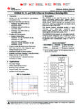
1 2011-2015 Microchip Technology 1 PIC16(L)F1503 High-Performance RISC CPU: C Compiler Optimized Architecture Only 49 Instructions Operating Speed:- DC 20 MHz clock input- DC 200 ns instruction cycle Interrupt Capability with Automatic Context Saving 16-Level Deep Hardware Stack with Optional Overflow/Underflow Reset Direct, Indirect and Relative Addressing modes:- Two full 16-bit File Select Registers (FSRs)- FSRs can read program and data memoryFlexible Oscillator Structure: 16 MHz Internal Oscillator Block:- Factory calibrated to 1%, typical- Software selectable frequency range from 16 MHz to 31 kHz 31 kHz Low-Power Internal Oscillator Three External Clock modes up to 20 MHzSpecial Microcontroller Features: Operating Voltage Range:- to (PIC16LF1503)- to (PIC16F1503) Self-Programmable under Software Control Power-on Reset (POR) Power-up Timer (PWRT) Programmable Low-Power Brown-out Reset (LPBOR) Extended Watchdog Timer (WDT).
2 - Programmable period from 1 ms to 256s Programmable Code Protection In-Circuit Serial Programming (ICSP ) via Two Pins Enhanced Low-Voltage Programming (LVP) In-Circuit Debug (ICD) via Two Pins Power-Saving Sleep mode:- Low-Power Sleep mode- Low-Power BOR (LPBOR) Integrated Temperature Indicator 128 Bytes High-Endurance Flash- 100,000 write Flash endurance (minimum)Memory: 2 Kwords Linear Program Memory Addressing 128 bytes Linear Data Memory Addressing High-Endurance Flash Data Memory (HEF)- 128 bytes if nonvolatile data storage- 100k erase/write cycleseXtreme Low-Power (XLP) Features (PIC16LF1503): Sleep Current:- 20 nA @ , typical Watchdog Timer Current:- 260 nA @ , typical Operating Current:-30 A/MHz @ , typicalPeripheral Features: Analog-to-Digital Converter (ADC):- 10-bit resolution- Eight external channels- Three internal channels:- Fixed Voltage Reference- Digital-to-Analog Converter (DAC)- Temperature Indicator channel- Auto acquisition capability- Conversion available during Sleep 5-Bit Digital-to-Analog Converter (DAC):- Output available externally- Positive reference selection- Internal connections to comparators and ADC Two Comparators.
3 - Rail-to-rail inputs- Power mode control- Software controllable hysteresis Voltage Reference:- Fixed Voltage Reference (FVR) with 1x, 2x and 4x Gain output levels 12 I/O Pins (1 Input-only Pin):- High current sink/source 25 mA/25 mA- Individually programmable weak pull-ups- Individually programmable Interrupt-on-Change (IOC) pins Timer0: 8-Bit Timer/Counter with 8-Bit Programmable Prescaler Enhanced Timer1:- 16-bit timer/counter with prescaler- External Gate Input mode Timer2: 8-Bit Timer/Counter with 8-Bit Period Register, Prescaler and Postscaler Four 10-bit PWM modules Master Synchronous Serial Port (MSSP) with SPI and I2C with:- 7-bit address masking- SMBus/PMBus compatibility14-Pin Flash, 8-Bit MicrocontrollersPIC16(L)F1503DS40001607D -page 2 2011-2015 Microchip Technology Features (Continued): Two Configurable Logic Cell (CLC) modules.
4 - 16 selectable input source signals- Four inputs per module- Software control of combinational/sequential logic/state/clock functions- AND/OR/XOR/D Flop/D Latch/SR/JK- Inputs from external and internal sources- Output available to pins and peripherals- Operation while in Sleep Numerically Controlled Oscillator (NCO):- 20-bit accumulator- 16-bit increment- True linear frequency control- High-speed clock input- Selectable Output modes- Fixed Duty Cycle (FDC) mode- Pulse Frequency (PF) mode Complementary Waveform Generator (CWG):- Eight selectable signal sources- Selectable falling and rising edge dead-band control- Polarity control- Four auto-shutdown sources- Multiple input sources: PWM, CLC, NCOPIC12(L)F1501/PIC16(L)F150X FAMILY TYPESD eviceData Sheet IndexProgram MemoryFlash (words)Data SRAM(bytes)I/O s(2)10-bit ADC (ch)ComparatorsDACT imers(8/16-bit)PWMEUSARTMSSP (I2C/SPI)CWGCLCNCOD ebug(1)XLPPIC12(L)F1501(1)10246464112/14 121H PIC16(L)F1503 (2) 2048128128212/14 1121H PIC16(L)F1507(3)20481281812 2/14 121H PIC16(L)F1508(4)40962561812212/1411141I/ HYPIC16(L)F1509(4)81925121812212/1411141 I/HYNote 1:Debugging Methods: (I) - Integrated on Chip.
5 (H) - using Debug Header; (E) - using Emulation :One pin is Sheet Index: (Unshaded devices are described in this document.)1:DS40001615 PIC12(L)F1501 Data Sheet, 8-Pin Flash, 8-Bit :DS40001607 PIC16(L)F1503 Data Sheet, 14-Pin Flash, 8-Bit :DS40001586 PIC16(L)F1507 Data Sheet, 20-Pin Flash, 8-Bit :DS40001609 PIC16(L)F1508/9 Data Sheet, 20-Pin Flash, 8-Bit :For other small form-factor package availability and marking information, please or contact your local sales office. 2011-2015 Microchip Technology 3 PIC16(L)F1503 PIN DIAGRAMSPIC16(L)F15031234141312115671098 VDDRA5RA4 MCLR/VPP/RA3RC5RC4RC3 VSSRA0/ICSPDATRA1/ICSPCLKRA2RC0RC1RC2 Note:See Ta b l e 1 for location of all peripheral PDIP, SOIC, TSSOPNote 1:See Table 1 for location of all peripheral :It is recommended that the exposed bottom pad be connected to (L)F150316-pin QFN, UQFNPIC16(L)F1503DS40001607D-page 4 2011-2015 Microchip Technology ALLOCATION TABLETABLE 1.
6 14-Pin ALLOCATION TABLE (PIC16(L)F1503)I/O14-Pin PDIP/SOIC/TSSOP16-Pin QFN, UQFNADCR eferenceComparatorTimerCWGNCOCLCPWMMSSPI nterruptPull-UpBasicRA01312AN0 DACOUT1C1IN+ IOCYICSPDATRA11211AN1 VREF+C1IN0-C2IN0- IOCYICSPCLKRA21110AN2 DACOUT2C1 OUTT0 CKICWG1 FLT CLC1 PWM3 INTIOCY RA343 T1G(1) CLC1IN0 SS(1)IOCYMCLRVPPRA432AN3 T1G NCO1(1) SDO(1)IOCYCLKOUTRA521 T1 CKI NCO1 CLKCLC1IN1 IOCYCLKINRC0109AN4 C2IN+ CLC2 SCLSCK RC198AN5 C1IN1-C2IN1- NCO1 PWM4 SDASDI RC287AN6 C1IN2-C2IN2- SDO RC376AN7 C1IN3-C2IN3- CLC2IN0 PWM2SS RC465 C2 OUT CWG1B CLC2IN1 RC554 CWG1A CLC1(1)PWM1 VDD116 VDDVSS1413 VSSNote 1:Alternate pin function selected with the APFCON (Register 11-1) register.
7 2011-2015 Microchip Technology 5 PIC16(L)F1503 TABLE OF Overview .. Mid-Range CPU .. Organization .. Configuration .. Mode (Sleep) .. Timer (WDT) .. Flash Program Memory Control .. I/O Ports .. Interrupt-On-Change .. Fixed Voltage Reference (FVR) .. Temperature Indicator Module .. Analog-to-Digital Converter (ADC) Module .. 5-Bit Digital-to-Analog Converter (DAC) Module .. Comparator Timer0 Module .. Timer1 Module with Gate Timer2 Module .. Master Synchronous Serial Port (MSSP) Module .. Pulse-Width Modulation (PWM) Module .. Configurable Logic Cell (CLC).. Numerically Controlled Oscillator (NCO) Module.
8 Complementary Waveform Generator (CWG) Module .. In-Circuit Serial Programming (ICSP ) .. Instruction Set Summary .. Electrical DC and AC Characteristics Graphs and Charts .. Development Packaging 332 Appendix A: Data Sheet Revision 347 The Microchip Website .. 348 Customer Change Notification Service .. 348 Customer Support .. 348 Product Identification System .. 349 PIC16(L)F1503DS40001607D-page 6 2011-2015 Microchip Technology OUR VALUED CUSTOMERSIt is our intention to provide our valued customers with the best documentation possible to ensure successful use of your Microchipproducts. To this end, we will continue to improve our publications to better suit your needs.
9 Our publications will be refined andenhanced as new volumes and updates are introduced. If you have any questions or comments regarding this publication, please contact the Marketing Communications Department viaE-mail at or fax the Reader Response Form in the back of this data sheet to (480) 792-4150. Wewelcome your Current Data SheetTo obtain the most up-to-date version of this data sheet, please register at our Worldwide Website at: can determine the version of a data sheet by examining its literature number found on the bottom outside corner of any last character of the literature number is the version number, ( , DS30000A is version A of document DS30000).
10 ErrataAn errata sheet, describing minor operational differences from the data sheet and recommended workarounds, may exist for currentdevices. As device/documentation issues become known to us, we will publish an errata sheet. The errata will specify the revisionof silicon and revision of document to which it determine if an errata sheet exists for a particular device, please check with one of the following: Microchip s Worldwide Website; Your local Microchip sales office (see last page)When contacting a sales office, please specify which device, revision of silicon and data sheet (include literature number) you Notification SystemRegister on our website at to receive the most current information on all of our products.