Transcription of 8/14-Pin Flash Microcontrollers with XLP Technology
1 2010-2015 Microchip Technology 1 High-Performance RISC CPU Only 49 Instructions to Learn:- All single-cycle instructions except branches Operating Speed:- DC 32 MHz oscillator/clock input- DC 125 ns instruction cycle Interrupt Capability with Automatic Context Saving 16-Level Deep Hardware Stack with Optional Overflow/Underflow Reset Direct, Indirect and Relative Addressing modes:- Two full 16-bit File Select Registers (FSRs)- FSRs can read program and data memoryFlexible Oscillator Structure Precision 32 MHz internal Oscillator Block:- Factory calibrated to 1%, typical- Software selectable frequencies range of 31 kHz to 32 MHz 31 kHz Low-Power Internal Oscillator Four Crystal modes up to 32 MHz Three External Clock modes up to 32 MHz 4X Phase Lock Loop (PLL) Fail-Safe Clock Monitor:- Allows for safe shutdown if peripheral clock stops Two-Speed Oscillator Start-up Reference Clock module:- Programmable clock output frequency and duty-cycleSpecial Microcontroller Features Full Operation PIC12F1822/16F1823 Operation PIC12LF1822/16LF1823 Self-Reprogrammable under Software Control Power-on Reset (POR), Power-up Timer (PWRT) and Oscillator Start-up Timer (OST) Programmable Brown-out Reset (BOR) Extended Watchdog Timer (WDT) In-Circuit Serial Programming (ICSP ) via Two Pins In-Circuit Debug (ICD) via Two Pins Enhanced Low-Voltage Programming (LVP) Operating Voltage Range:- (PIC12F1822/16F1823)- (PIC12LF1822/16LF1823) Programmable Code Protection Self-Programmable under Software ControlExtreme Low-Power Management PIC12LF1822/16LF1823 with XLP Sleep mode: 20 nA @ , typical Watchdog Timer: 300 nA @ , typical Timer1 Oscillator.
2 650 nA @ 32 kHz, typical Operating Current: 30 A/MHz @ , typicalAnalog Features Analog-to-Digital Converter (ADC) module:- 10-bit resolution, up to 8 channels- Conversion available during Sleep Analog Comparator module:- Up to two rail-to-rail analog comparators- Power mode control- Software controllable hysteresis Voltage Reference module:- Fixed Voltage Reference (FVR) with , and output levels- 5-bit rail-to-rail resistive DAC with positive and negative reference selectionPeripheral Highlights Up to 11 I/O Pins and 1 Input-Only Pin:- High current sink/source 25 mA/25 mA- Programmable weak pull-ups- Programmable interrupt-on-change pins Timer0: 8-Bit Timer/Counter with 8-Bit Prescaler Enhanced Timer1:- 16-bit timer/counter with prescaler- External Gate Input mode- Dedicated, low-power 32 kHz oscillator driver Timer2: 8-Bit Timer/Counter with 8-Bit PeriodRegister, Prescaler and Postscaler Enhanced CCP (ECCP) modules:- Software selectable time bases- Auto-shutdown and auto-restart- PWM steering Master Synchronous Serial Port (MSSP) with SPI and I2 CTM with:- 7-bit address masking- SMBus/PMBusTM compatibility Enhanced Universal Synchronous Asynchronous Receiver Transmitter (EUSART) module:- RS-232, RS-485 and LIN compatible- Auto-Baud Detect Capacitive Sensing (CPS) module (mTouch ):- Up to 8 input channelsPIC12(L)F1822/16(L)F18238/14-Pin Flash Microcontrollers with XLP TechnologyPIC12(L)F1822/16(L)F1823DS4000 1413E-page 2 2010-2015 Microchip Technology Features (Continued) Data Signal Modulator module- Selectable modulator and carrier sources SR Latch:- Multiple Set/Reset input options- Emulates 555 Timer applicationsTABLE 1.
3 PIC12(L)F1822/1840/PIC16(L)F182X/1847 FAMILY TYPESD eviceData Sheet IndexProgram MemoryFlash (words)Data EEPROM(bytes)Data SRAM(bytes)I/O s(2)10-bit ADC (ch)CapSense (ch)ComparatorsTimers(8/16-bit)EUSARTMSS P (I2C /SPI)ECCP (Full-Bridge)ECCP (Half-Bridge)CCPSR LatchDebug(1)XLPPIC12(L)F1822(1)2K256128 64412/1110/1/0YI/HYPIC12(L)F1840(2)4K256 25664412/1110/1/0YI/HYPIC16(L)F1823(1)2K 256128128822/1111/0/0YI/HYPIC16(L)F1824( 3)4K256256128824/1111/1/2YI/HYPIC16(L)F1 825(4)8K2561024128824/1111/1/2YI/HYPIC16 (L)F1826(5)2K25625616121222/1111/0/0YI/H YPIC16(L)F1827(5)4K25638416121224/1121/1 /2YI/HYPIC16(L)F1828(3)4K25625618121224/ 1111/1/2YI/HYPIC16(L)F1829(4)8K256102418 121224/1121/1/2YI/HYPIC16(L)F1847(6)8K25 6102416121224/1121/1/2YI/HYNote 1:I - Debugging, Integrated on Chip; H - Debugging, available using Debug :One pin is Sheet Index: (Unshaded devices are described in this document.)1:DS41413 PIC12(L)F1822/PIC16(L)F1823 Data Sheet, 8/14-Pin Flash :DS41441 PIC12(L)F1840 Data Sheet, 8-Pin Flash :DS41419 PIC16(L)F1824/1828 Data Sheet, 28/40/44-Pin Flash :DS41440 PIC16(L)F1825/1829 Data Sheet, 14/20-Pin Flash :DS41391 PIC16(L)F1826/1827 Data Sheet, 18/20/28-Pin Flash :DS41453 PIC16(L)F1847 Data Sheet, 18/20/28-Pin Flash :For other small form-factor package availability and marking information, please visit or contact your local sales office.
4 2010-2015 Microchip Technology 3 PIC12(L)F1822/16(L)F1823 FIGURE 1:8-PIN DIAGRAM FOR PIC12(L)F1822 TABLE 2:8-PIN ALLOCATION TABLE (PIC12(L)F1822)I/O8-Pin PDIP/SOIC/DFN/UDFNA/DReferenceCap SenseComparatorSR LatchTimersECCPEUSARTMSSPI nterruptModulatorPull-upBasicRA07AN0 DACOUTCPS0C1IN+ P1B(1)TX(1)CK(1)SDO(1)SS(1)IOCMDOUTYICSP DATICDDATRA16AN1 VREF+CPS1 C1IN0-SRI RX(1)DT(1)SCLSCKIOCMDMINYICSPCLKICPCLKRA 25AN2 CPS2C1 OUTSRQT0 CKICCP1(1)P1A(1)FLT0 SDASDIINT/IOCMDCIN1Y RA34 T1G(1) SS(1)IOC YMCLRVPPRA43AN3 CPS3C1IN1- T1G(1)T1 OSOP1B(1)TX(1)CK(1)SDO(1)IOCMDCIN2 YOSC2 CLKOUTCLKRRA52 SRNQT1 CKIT1 OSICCP1(1)P1A(1)RX(1)DT(1) IOC YOSC1 CLKINVDD1 VDDVSS8 VSSNote 1:Pin function is selectable via the APFCON , SOIC, DFN, UDFN12348765 VDDRA5RA4 MCLR/VPP/RA3 VSSRA0/ICSPDATRA1/ICSPCLKRA2 PIC12(L)F1822 PIC12(L)F1822/16(L)F1823DS40001413E-page 4 2010-2015 Microchip Technology 2:14-PIN DIAGRAM FOR PIC16(L)F1823 FIGURE 3:16-PIN DIAGRAM FOR PIC16(L)F1823 PDIP, SOIC, TSSOPPIC16(L)F18231234141312115671098 VDDRA5RA4 MCLR/VPP/RA3RC5RC4RC3 VSSRA0/ICSPDATRA1/ICSPCLKRA2RC0RC1RC2123 49101112567816151413 PIC16(L)F1823 VDDNCNCVSSRA5RA4 MCLR/VPP/RA3RC5RA0/ICSPDATRA1/ICSPCLKRA2 RC0RC4RC3RC2RC1 QFN, UQFN 2010-2015 Microchip Technology 5 PIC12(L)F1822/16(L)F1823 TABLE 3.
5 14-PIN ALLOCATION TABLE (PIC16(L)F1823)I/O14-Pin PDIP/SOIC/TSSOP16-Pin QFN/UQFNA/DReferenceCap SenseComparatorSR LatchTimersECCPEUSARTMSSPI nterruptModulatorPull-upBasicRA01312AN0 DACOUTCPS0C1IN+ TX(1)CK(1) IOC YICSPDATICDDATRA112 11AN1 VREF+CPS1C12IN0-SRI RX(1)DT(1) IOC YICSPCLKICDCLKRA21110AN2 CPS2C1 OUTSRQT0 CKIFLT0 INT/IOC Y RA343 T1G(1) SS(1)IOC YMCLRVPPRA432AN3 CPS3 T1G(1)T1 OSO SDO(1)IOC YOSC2 CLKOUTCLKRRA521 T1 CKIT1 OSI IOC YOSC1 CLKINRC0109AN4 CPS4C2IN+ SCLSCK Y RC198AN5 CPS5C12IN1- SDASDI Y RC287AN6 CPS6C12IN2- P1D SDO(1) MDCIN1Y RC376AN7 CPS7C12IN3- P1C SS(1) MDMINY RC465 C2 OUTSRNQ P1 BTX(1)CK(1) MDOUTY RC554 CCP1P1 ARX(1)DT(1) MDCIN2Y VDD116 VDDVSS1413 VSSNote 1:Pin function is selectable via the APFCON (L)F1822/16(L)F1823DS40001413E-page 6 2010-2015 Microchip Technology of Overview .. Mid-Range CPU .. Organization .. Configuration.
6 Module (With Fail-Safe Clock Monitor).. Clock Module .. Mode (Sleep) .. Watchdog Timer .. Data EEPROM and Flash Program Memory Control .. I/O Ports .. Interrupt-On-Change .. Fixed Voltage Reference (FVR) .. Temperature Indicator Module .. Analog-to-Digital Converter (ADC) Module .. Digital-to-Analog Converter (DAC) Module .. SR Comparator Timer0 Module .. Timer1 Module with Gate Timer2 Module .. Data Signal Modulator .. Capture/Compare/PWM Modules .. Master Synchronous Serial Port Module .. Enhanced Universal Synchronous Asynchronous Receiver Transmitter (EUSART) .. Capacitive Sensing (CPS) Module .. In-Circuit Serial Programming (ICSP ) .. Instruction Set Summary .. Electrical DC and AC Characteristics Graphs and Charts .. Development Packaging 391 Appendix A: Data Sheet Revision History .. 418 Appendix B: Migrating From Other PIC Devices.
7 418 The Microchip Web Site .. 419 Customer Change Notification Service .. 419 Customer Support .. 419 Product Identification 420 2010-2015 Microchip Technology 7 PIC12(L)F1822/16(L)F1823TO OUR VALUED CUSTOMERSIt is our intention to provide our valued customers with the best documentation possible to ensure successful use of your Microchipproducts. To this end, we will continue to improve our publications to better suit your needs. Our publications will be refined andenhanced as new volumes and updates are introduced. If you have any questions or comments regarding this publication, please contact the Marketing Communications Department viaE-mail at We welcome your Current Data SheetTo obtain the most up-to-date version of this data sheet, please register at our Worldwide Web site at: can determine the version of a data sheet by examining its literature number found on the bottom outside corner of any last character of the literature number is the version number, ( , DS30000000A is version A of document DS30000000).
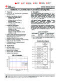
8 ErrataAn errata sheet, describing minor operational differences from the data sheet and recommended workarounds, may exist for currentdevices. As device/documentation issues become known to us, we will publish an errata sheet. The errata will specify the revisionof silicon and revision of document to which it determine if an errata sheet exists for a particular device, please check with one of the following: Microchip s Worldwide Web site; Your local Microchip sales office (see last page)When contacting a sales office, please specify which device, revision of silicon and data sheet (include literature number) you Notification SystemRegister on our web site at to receive the most current information on all of our (L)F1822/16(L)F1823DS40001413E-page 8 2010-2015 Microchip Technology OVERVIEWThe PIC12(L)F1822/16(L)F1823 are described within thisdata sheet. They are available in 8/14 pin 1-1 shows a block diagram of thePIC12(L)F1822/16(L)F1823 devices.
9 Tables1-2 and1-3show the pinout Ta b l e 1 - 1 for peripherals available 1-1:DEVICE PERIPHERAL SUMMARYP eripheral PIC12(L)F1822 PIC16(L)F1823 ADC Capacitive Sensing (CPS) Module Data EEPROM Digital-to-Analog Converter (DAC) Digital Signal Modulator (DSM) EUSART Fixed Voltage Reference (FVR) SR Latch Capture/Compare/PWM ModulesECCP1 ComparatorsC1 C2 Master Synchronous Serial PortsMSSP TimersTimer0 Timer1 Timer2 2010-2015 Microchip Technology 9 PIC12(L)F1822/16(L)F1823 FIGURE 1-1:PIC12(L)F1822/16(L)F1823 BLOCK DIAGRAMPORTAEUSARTC omparatorsMSSPT imer1 Timer0 ECCP1 ADC10-BitPORTC(3)SRLatchNote1:See applicable chapters for more information on :See Ta b l e 1 - 1 for peripherals available on specific :PIC16(L)F1823 MemoryEEPROMRAMT imingGenerationINTRCO scillatorMCLR(Figure 2-1)ModulatorCapSenseClockCLKRR eferenceDACFVROSC1/CLKINOSC2/CLKOUTPIC12 (L)F1822/16(L)F1823DS40001413E-page 10 2010-2015 Microchip Technology 1-2.
10 PIC12(L)F1822 PINOUT DESCRIPTIONNameFunctionInput TypeOutput TypeDescriptionRA0/AN0/CPS0/C1IN+/DACOUT /TX(1)/CK(1)/SDO(1)/SS(1)/P1B(1)/MDOUT/I CSPDAT/ICDDATRA0 TTLCMOS General purpose A/D Channel 0 Capacitive sensing input +AN Comparator C1 positive ANDigital-to-Analog Converter CMOS USART asynchronous USART synchronous CMOS SPI data Slave Select CMOS PWM CMOS Modulator ICSP Data +/C1IN0-/SRI/RX(1)/DT(1)/SCL/SCK/MDMIN/I CSPCLK/ICDCLKRA1 TTLCMOS General purpose A/D Channel 1 Capacitive sensing input +AN A/D and DAC Positive Voltage Reference Comparator C1 or C2 negative SR latch USART asynchronous USART synchronous ODI2C SPI Modulator source Serial Programming (1)/P1A(1)/FLT0/SDA/SDI/INT/MDCIN1RA2 STCMOS General purpose A/D Channel 2 Capacitive sensing input CMOS Comparator C1 CMOS SR latch non-inverting Timer0 clock Capture/Compare/PWM CMOS PWM ECCP Auto-Shutdown Fault ODI2C data SPI data External Modulator Carrier Input (1)/T1G(1)/VPP/MCLRRA3 TTL General purpose Slave Select Timer1 Gate Programming Master Clear with internal :AN = Analog input or output CMOS = CMOS compatible input or outputOD= Open DrainTTL = TTL compatible inputST= Schmitt Trigger input with CMOS levels I2C = Schmitt Trigger input with I2C HV = High VoltageXTAL = CrystallevelsNote 1:Pin functions can be assigned to one of two pin locations via software.