Transcription of 1A, 76V, High-Efficiency MAXPower Step-Down DC-DC …
1 AVAILABLEF unctional DiagramsPin Configurations appear at end of data Diagrams continued at end of data is a trademark of Maxim Integrated Products, pricing, delivery, and ordering information, please contact Maxim Direct at 1-888-629-4642, or visit Maxim s website at KIT AVAILABLEG eneral DescriptionThe MAX5035 easy-to-use, High-Efficiency , high-volt-age, Step-Down DC-DC converter operates from aninput voltage up to 76V and consumes only 270 A qui-escent current at no load. This pulse-width modulated(PWM) converter operates at a fixed 125kHz switchingfrequency at heavy loads, and automatically switchesto pulse-skipping mode to provide low quiescent cur-rent and high efficiency at light loads. The MAX5035includes internal frequency compensation simplifyingcircuit implementation. The device uses an internal low-on-resistance, high-voltage, DMOS transistor to obtainhigh efficiency and reduce overall system cost.
2 Thisdevice includes undervoltage lockout, cycle-by-cyclecurrent limit, hiccup mode output short-circuit protec-tion, and thermal MAX5035 delivers up to 1A output current. The out-put current may be limited by the maximum power dis-sipation capability of the package. External shutdown isincluded, featuring 10 A (typ) shutdown current. TheMAX5035A/B/C versions have fixed output voltages , 5V, and 12V, respectively, while the MAX5035D/Eversions have an adjustable output voltage from MAX5035 is available in space-saving 8-pin SOand 8-pin plastic DIP packages and operates over theautomotive (-40 C to +125 C) temperature ElectronicsIndustrialDistributed PowerFeatures Wide to 76V Input Voltage Range Fixed ( , 5V, 12V) and Adjustable ( to ) Versions 1A Output Current Efficiency Up to 94% Internal High-Side DMOS FET 270 A Quiescent Current at No Load, 10 AShutdown Current Internal Frequency Compensation Fixed 125kHz Switching Frequency Thermal Shutdown and Short-Circuit CurrentLimit 8-Pin SO and PDIP Packages1A, 76V, High-Efficiency MAXP ower Step-Down DC-DC ConverterOrdering Information19-2988; Rev 5.
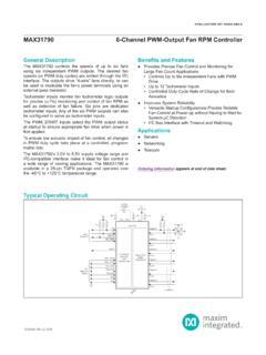
3 5/11 PARTTEMP RANGEPIN-PACKAGEOU TPU TVO LTA GE( V)MAX5035 AUSA0 C to +85 C8 SOMAX5035 AUPA0 C to +85 C8 PDIPMAX5035 AASA-40 C to +125 C 8 SOM AX 5035 AAS A/V + -40 C to +125 C 8 C to +85 C8 SOMAX5035 BUPA0 C to +85 C8 PDIPMAX5035 BASA-40 C to +125 C 8 SOM AX 5035 BAS A/V + -40 C to +125 C 8 VIEWVINGNDON/OFFMAX5035SO/PDIPPin ConfigurationMAX5035 GNDBSTLXVINSGNDFBD150SQ100VD100 TO 76V68 F68 FONOFFR1R2ON/OFFT ypical Operating Circuit/V denotes an automotive qualified part.+Denotes a lead(Pb)-free/RoHS-compliant Information continued at end of data Information1A, 76V, High-Efficiency MAXP ower Step-Down DC-DC ConverterABSOLUTE MAXIMUM RATINGSS tresses beyond those listed under Absolute Maximum Ratings may cause permanent damage to the device. These are stress ratings only, and functionaloperation of the device at these or any other conditions beyond those indicated in the operational sections of the specifications is not implied.
4 Exposure toabsolute maximum rating conditions for extended periods may affect device reliability.(Voltages referenced to GND, unless otherwise specified.) to +80 VSGND .. to + to (VIN+ )BST .. to (VIN+ 10V)BST (transient < 100ns) .. to (VIN+ 15V)BST to to +10 VBST to LX (transient < 100ns) .. to +15 to + to +12 VFBMAX5035A/MAX5035B/MAX5035C .. to +15 VMAX5035D/E .. to +12 VVOUTS hort-Circuit Duration (VIN 40V)..IndefiniteVD Short-Circuit Duration ..IndefiniteContinuous Power Dissipation (TA= +70 C)8-Pin PDIP (derate C above +70 C)..727mW8-Pin SO (derate C above +70 C)..471mWOperating Temperature RangeMAX5035_U_ _ ..0 C to +85 CMAX5035_A_ _ ..-40 C to +125 CStorage Temperature Range ..-65 C to +150 CJunction Temperature ..+150 CLead Temperature (soldering, 10s) ..+300 CSoldering Temperature (reflow)Lead(Pb) +260 CContaining lead(Pb) ..+240 CELECTRICAL CHARACTERISTICS (MAX5035_U_ _)(VIN= +12V, VON/OFF= +12V, IOUT= 0, TA= 0 C to +85 C, unless otherwise noted.)
5 Typical values are at TA= +25 C. See theTypical Application Circuit.) Voltage RangeVINMAX5035 = to 76V,IOUT = 20mA to = to 76V,IOUT = 20mA to VoltageVOUTMAX5035 CVIN = 15V to 76V,IOUT = 20mA to = to 76V, MAX5035 VoltageVFBVIN = to 76V, = 12V, ILOAD = , MAX5035A86 VIN = 12V, ILOAD = , MAX5035B90 VIN = 24V, ILOAD = , MAX5035C94 Efficiency VIN = 12V, VOUT = 5V, ILOAD = ,MAX5035D/E90%VFB = , VIN = to 76V, MAX5035A270440 VFB = , VIN = to 76V, MAX5035B270440 VFB = 13V, VIN = 15V to 76V, MAX5035C270440 VFB = , MAX5035D270440 Quiescent Supply CurrentIQVFB = , MAX5035E340460 AShutdown CurrentISHDNVON/OFF = 0V, VIN = to 76V1045 APeak Switch Current LimitILIM(Note 1) Integrated1A, 76V, High-Efficiency MAXP ower Step-Down DC-DC ConverterELECTRICAL CHARACTERISTICS (continued) (MAX5035_U_ _)(VIN= +12V, VON/OFF= +12V, IOUT= 0, TA= 0 C to +85 C, unless otherwise noted. Typical values are at TA= +25 C. See theTypical Application Circuit.
6 PARAMETERSYMBOLCONDITIONSMINTYPMAXUNITSS witch Leakage CurrentIOLVIN = 76V, VON/OFF = 0V, VLX = ASwitch On-ResistanceRDS(ON)ISWITCH = PFM ThresholdIPFMM inimum switch current in any cycle5585130mAFB Input Bias CurrentIBMAX5035D/E-150+ +150nAON/OFF CONTROL INPUTR ising trip point for MAX5035A/B/ Input-Voltage ThresholdVON/OFFR ising trip point for Input-Voltage HysteresisVHYST100mVON/OFF Input CurrentION/OFFVON/OFF = 0V to VIN10150nAON/OFF Operating VoltageRangeVON/OFF76 VOSCILLATORO scillator FrequencyfOSC109125135kHzMaximum Duty CycleDMAXMAX5035D/E95%VOLTAGE REGULATORR egulator Output VoltageVDVIN = to 76V, IL = VIN , IL = Regulation VD/ IVD0 to 5mA150 PACKAGE THERMAL CHARACTERISTICSSO package (JEDEC 51)170 Thermal Resistance(Junction to Ambient) JADIP package (JEDEC 51)110 C/WTHERMAL SHUTDOWNT hermal-Shutdown JunctionTemperatureTSH+160 CThermal-Shutdown HysteresisTHYST20 CELECTRICAL CHARACTERISTICS (MAX5035_A_ _)(VIN= +12V, VON/OFF= +12V, IOUT= 0, TA= TJ= -40 C to +125 C, unless otherwise noted.)
7 Typical values are at TA= +25 C. Seethe Typical Application Circuit.) (Note 2) Voltage RangeVINMAX5035 = to 76V,IOUT = 20mA to = to 76V,IOUT = 20mA to VoltageVOUTMAX5035 CVIN = 15V to 76V,IOUT = 20mA to Integrated31A, 76V, High-Efficiency MAXP ower Step-Down DC-DC ConverterELECTRICAL CHARACTERISTICS (MAX5035_A_ _) (continued)(VIN= +12V, VON/OFF= +12V, IOUT= 0, TA= TJ= -40 C to +125 C, unless otherwise noted. Typical values are at TA= +25 C. Seethe Typical Application Circuit.) (Note 2)PARAMETERSYMBOLCONDITIONSMINTYPMAXUNIT SVIN = to 76V, VoltageVFBVIN = to 76V, = 12V, ILOAD = , MAX5035A86 VIN = 12V, ILOAD = , MAX5035B90 VIN = 24V, ILOAD = , MAX5035C94 Efficiency VIN = 12V, VOUT = 5V, ILOAD = ,MAX5035D/E90%VFB = , VIN = to 76V, MAX5035A270440 VFB = , VIN = to 76V, MAX5035B270440 VFB = 13V, VIN = 15V to 76V, MAX5035C270440 VFB = , MAX5035D270440 Quiescent Supply CurrentIQVFB = , MAX5035E340460 AShutdown CurrentISHDNVON/OFF = 0V, VIN = to 76V1045 APeak Switch Current LimitILIM(Note 1) = 76V, VON/OFF = 0V, VLX = 0V1 Switch Leakage CurrentIOLVIN = 76V, VON/OFF = 0V, VLX = 0V,MAX5035E5 ASwitch On-ResistanceRDS(ON)
8 ISWITCH = PFM ThresholdIPFMM inimum switch current in any cycle5585130mAFB Input Bias CurrentIBMAX5035D/E-150+ +150nAON/OFF CONTROL INPUTR ising trip point for MAX5035A/B/ Input-Voltage ThresholdVON/OFFR ising trip point for Input-Voltage HysteresisVHYST100mVON/OFF Input CurrentION/OFFVON/OFF = 0V to VIN10150nAON/OFF Operating VoltageRangeVON/OFF76 VOSCILLATORO scillator FrequencyfOSC105125137kHzMaximum Duty CycleDMAXMAX5035D/E95%VOLTAGE REGULATORR egulator Output VoltageVDVIN = to 76V, IL = VIN , IL = Regulation VD/ IVD0 to 5mA150 MAX50354 Maxim Integrated1A, 76V, High-Efficiency MAXP ower Step-Down DC-DC ConverterTypical Operating Characteristics(VIN= 12V, VON/OFF= 12V, TA= -40 C to +125 C, unless otherwise noted. Typical values are at TA= +25 C. See the TypicalApplication Circuit, if applicable.)PARAMETERSYMBOLCONDITIONSMIN TYPMAXUNITSPACKAGE THERMAL CHARACTERISTICSSO package (JEDEC 51)170 Thermal Resistance(Junction to Ambient) JADIP package (JEDEC 51)110 C/WTHERMAL SHUTDOWNT hermal-Shutdown JunctionTemperatureTSH+160 CThermal-Shutdown HysteresisTHYST20 CNote 1:Switch current at which current limit is 2:All limits at -40 C are guaranteed by design, not production vs.
9 TEMPERATURE(MAX5035 AASA, VOUT = )MAX5035 toc01 TEMPERATURE ( C)VOUT (V) = = 1A100500-50150-252575125 VOUT vs. TEMPERATURE(MAX5035 DASA, VOUT = 5V)MAX5035 toc02 TEMPERATURE ( C)VOUT (V) = = 1 ALINE REGULATION(MAX5035 AASA, VOUT = )MAX5035 toc03 INPUT VOLTAGE (V)OUTPUT VOLTAGE (V) = 1 AIOUT = REGULATION(MAX5035 DASA, VOUT = 5V)MAX5035 toc04 INPUT VOLTAGE (V)OUTPUT VOLTAGE (V) = 1 AIOUT = REGULATION(MAX5035 AASA, VOUT = )MAX5035 toc05 ILOAD (mA)VOUT (V) = , 24 VVIN = 76 VLOAD REGULATION(MAX5035 DASA, VOUT = 5V)MAX5035 toc06 ILOAD (mA)VOUT (V) = 76 VVIN = 24 VVIN = CHARACTERISTICS (MAX5035_A_ _) (continued)(VIN= +12V, VON/OFF= +12V, IOUT= 0, TA= TJ= -40 C to +125 C, unless otherwise noted. Typical values are at TA= +25 C. Seethe Typical Application Circuit.) (Note 2)MAX5035 Maxim Integrated51A, 76V, High-Efficiency MAXP ower Step-Down DC-DC ConverterTypical Operating Characteristics (continued)(VIN= 12V, VON/OFF= 12V, TA= -40 C to +125 C, unless otherwise noted.)
10 Typical values are at TA= +25 C. See the TypicalApplication Circuit, if applicable.)OUTPUT CURRENT LIMIT vs. TEMPERATUREMAX5035 toc10 TEMPERATURE ( C)OUTPUT CURRENT LIMIT (A) = 5V5% DROP IN VOUTOUTPUT CURRENT LIMITvs. INPUT VOLTAGEMAX5035 toc11 INPUT VOLTAGE (V)OUTPUT CURRENT LIMIT (A) = 5V5% DROP IN VOUTQUIESCENT SUPPLY CURRENTvs. TEMPERATUREMAX5035 toc12 TEMPERATURE ( C)QUIESCENT SUPPLY CURRENT ( A)230260290320350200100500-50150-2525751 25 QUIESCENT SUPPLY CURRENTvs. INPUT VOLTAGEMAX5035 toc13 INPUT VOLTAGE (V)QUIESCENT SUPPLY CURRENT ( A)665646362616230260290320350200676 SHUTDOWN CURRENTvs. TEMPERATUREMAX5035 toc14 TEMPERATURE ( C)SHUTDOWN CURRENT ( A)5101520250100500-50150-252575125 SHUTDOWN CURRENT vs. INPUT VOLTAGEMAX5035 toc15 INPUT VOLTAGE (V)SHUTDOWN CURRENT ( A)665646362616481216200676 EFFICIENCY vs. LOAD CURRENT(MAX5035 AASA, VOUT = )MAX5035 toc07 LOAD CURRENT (mA)EFFICIENCY (%)8006004002001020304050607080901000010 00 VIN = 76 VVIN = 48 VVIN = 24 VVIN = 12 VVIN = vs.