Transcription of 1A LOW DROPOUT ADJUSTABLE AND FIXED ... - Diodes …
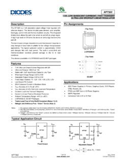
1 NOT RECOMMENDED FOR NEW DESIGN - USE AP7361C. AP7361. 1A LOW DROPOUT ADJUSTABLE AND FIXED -MODE REGULATOR WITH ENABLE. Description Pin Assignments The AP7361 is a 1A, ADJUSTABLE and FIXED output voltage, ultra-low (Top View). DROPOUT linear regulator with enable. The device includes pass element, error amplifier, band-gap reference, current limit and thermal OUT 1 8 IN. shutdown circuitry. The device is turned on when the EN pin is set to NC 2 7 NC. logic high level. GND. ADJ/NC 3 6 NC. The characteristics of the low DROPOUT voltage and low quiescent GND 4 5 EN. current make it suitable for low to medium power applications, for U-DFN3030-8. example, laptop computers, audio and video applications, and battery powered devices. The typical quiescent current is approximately ( Top View ) ( Top View ). 70 A. Built-in current-limit and thermal-shutdown functions prevent IC from damage in fault conditions. 3 3. The AP7361 is available in U-DFN3030-8, SOT89-5, SOT223, TO252 2 2 2. and SO-8EP package.
2 1 1. Features SOT223/SOT223R TO252/TO252R. Wide input voltage range: - 6V. (Top View). 150mV Very Low DROPOUT at 300mA Load (Top View). 500mV Very Low DROPOUT at 1A Load OUT 1 8 IN. EN 1 5 OUT. Low Quiescent Current (IQ): 70 A Typical EN 2 7 NC. ADJUSTABLE Output Voltage Range: 1V to GND 2 GND 3 6 NC. NC. FIXED Output Options: 1V to GND 4 5 NC. Very-Fast Transient Response ADJ/NC 3 4 IN. High PSRR SOT89-5 SO-8EP. Accurate Voltage Regulation Current Limiting and Short Circuit Protection Thermal Shutdown Protection Applications Stable with Ceramic Output Capacitor F Servers and Laptops Ambient Temperature Range -40 C to +85 C FPGA and DSP Core or I/O power U-DFN3030-8, SOT89-5, SOT223/SOT223R, TO252/TO252R TV, and Home Electrical Appliances and SO-8EP Battery-Powered Devices Available in Green Molding Compound (No Br, Sb). Totally Lead-Free & Fully RoHS Compliant (Notes 1 & 2). Halogen and Antimony Free. Green Device (Note 3). Notes: 1. No purposely added lead. Fully EU Directive 2002/95/EC (RoHS) & 2011/65/EU (RoHS 2) compliant.
3 2. See for more information about Diodes Incorporated's definitions of Halogen- and Antimony-free, "Green". and Lead-free. 3. Halogen- and Antimony-free "Green products are defined as those which contain <900ppm bromine, <900ppm chlorine (<1500ppm total Br + Cl) and <1000ppm antimony compounds. AP7361 1 of 22 March 2017. Document number: DS33626 Rev. 11 - 3 Diodes Incorporated AP7361. Typical Applications Circuit VIN VOUT VIN VOUT. IN OUT IN OUT. AP7361 AP7361 R1. 1uF 1uF Enable Enable EN EN ADJ. GND GND. R2. FIXED Version ADJUSTABLE Output U-DFN3030-8, SOT89-5 and SO-8EP U-DFN3030-8 and SOT89-5. VIN VOUT. IN OUT. AP7361. 1uF GND. FIXED Version TO252, SOT223. Pin Descriptions Pin Pin Number Function Name U-DFN3030-8 SOT89-5 TO252 TO252R SOT223 SOT223R SO-8EP. The input of the regulator. Bypass to ground through at IN 8 4 1 3 1 3 8. least 1 F ceramic capacitor. The output of the regulator. Bypass to ground through OUT 1 5 3 2 3 2 1 at least F ceramic capacitor. For improved ac load response a larger capacitor is recommended.
4 GND 4 2 2 1 2 1 4 Ground ADJUSTABLE voltage version only a resistor divider from ADJ 3 3 NA NA NA NA NA this pin to the OUT pin and ground sets the output voltage. EN 5 1 NA NA NA NA 2 Enable input, active high NC 2, 6, 7 NA NA NA NA NA 3, 5, 6, 7 No connection AP7361 2 of 22 March 2017. Document number: DS33626 Rev. 11 - 3 Diodes Incorporated AP7361. Functional Block Diagram IN OUT IN OUT. Current Limit Current Limit Gate Gate EN Driver and Thermal EN Driver and Thermal Shutdown R Shutdown ADJ. R. GND GND. FIXED Version U-DFN3030-8, SOT89-5 and SO-8EP ADJUSTABLE Version U-DFN3030-8 and SOT89-5. IN OUT. Current Limit Gate and Thermal Driver Shutdown R. R. GND. FIXED Version TO252, SOT223. AP7361 3 of 22 March 2017. Document number: DS33626 Rev. 11 - 3 Diodes Incorporated AP7361. Absolute Maximum Ratings (@TA = +25 C, unless otherwise specified.). Symbol Parameter Ratings Unit ESD HBM Human Body Model ESD Protection >2 KV. ESD MM Machine Model ESD Protection (Note 5) > 200 V.
5 VIN Input Voltage V. OUT, ADJ, EN Voltage VIN + V. TJ Operating Junction Temperature Range -40 to +150 C. TST Storage Temperature Range -65 to +150 C. Internally limited by maximum junction PD power Dissipation (Note 4). temperature of +150 C. U-DFN3030-8 1,700. TO252 1,250. PD power Dissipation (Note 4) SOT223 1,100 mW. SOT89-5 800. SO-8EP 1,190. Notes: 4. Ratings apply to ambient temperature at +25 C. 5. ESD MM rating at 150V for EN pin. Stresses greater than the 'Absolute Maximum Ratings' specified above, may cause permanent damage to the device. These are stress ratings only;. functional operation of the device at these or any other conditions exceeding those indicated in this specification is not implied. Device reliability may be affected by exposure to absolute maximum rating conditions for extended periods of time. Recommended Operating Conditions (@TA = +25 C, unless otherwise specified.). Symbol Parameter Min Max Unit VIN Input Voltage V. IOUT Output Current (Note 6) 0 A.
6 TA Operating Ambient Temperature -40 +85 C. Note: 6. The device maintains a stable, regulated output voltage without a load current. When the output current is large, attention should be given to the limitation of the package power dissipation. AP7361 4 of 22 March 2017. Document number: DS33626 Rev. 11 - 3 Diodes Incorporated AP7361. Electrical Characteristics (@TA = +25 C, VIN = VOUT +1V, CIN = 1 F, COUT = F, VEN = VIN unless otherwise specified.). Symbol Parameter Test Conditions Min Typ Max Unit VREF FB Reference Voltage IOUT = 10mA, TA = +25 C V. IADJ ADJ Pin Leakage A. IQ Input Quiescent Current Enabled, IOUT = 0A 70 90 A. ISHDN Input Shutdown Current VEN = 0V, IOUT = 0A -1 1 A. IOUT = 100mA, TA = +25 C -1 1. VOUT Output Voltage Accuracy IOUT = 100mA, -40 C TA +85 C -2 2 %. Over VIN, IOUT, and TA -3 3. VOUT VIN = VOUT +1V to TA = +25 C Line Regulation %/V. VIN VOUT 6V, IOUT = 100mA -40 C TA +85 C IOUT from 1mA to 300mA %. VOUT / VOUT Load Regulation IOUT from 1mA to 1A %.
7 IOUT = 300mA 150 200. VDROPOUT DROPOUT Voltage (Note 7) IOUT = 500mA 250 350 mV. IOUT = 1A 500 700. VIL EN Input Logic Low Voltage 0 V. VIH EN Input Logic High Voltage VIN V. IEN EN Input Leakage VIN = 6V, VEN = 0V or 6V A. ILIMIT Current Limit VIN = VOUT +1V A. ISHORT Short-Circuit Current VIN = VOUT +1V, Output Voltage < 15% VOUT 200 mA. power supply rejection Ratio f = 1 KHz, IOUT = 100mA 60 65. PSRR dB. (Note 8) f = 10 KHz, IOUT = 100mA 45. tST Start-Up Time VOUT = 3V, COUT = 1 F, RL = 30 200 s VOUT. Output Voltage Temperature Coefficient IOUT = 100mA, -40 C TA +85 C 130 ppm/ C. TA VOUT. TSHDN Thermal Shutdown Threshold 150 C. THYS Thermal Shutdown Hysteresis 20 C. U-DFN3030-8 (Note 9) 70. TO252 (Note 9) 95. JA Thermal Resistance Junction-to-Ambient SOT223 (Note 9) 110 C/W. SOT89-5 (Note 9) 150. SO-8EP (Note 9) 100. Notes: 7. DROPOUT voltage is the voltage difference between the input and the output at which the output voltage drops 2% below its nominal value. This parameter only applies to output voltages above since minimum V IN = 8.
8 For VIN and VIN = VOUT +1V. For VIN < , the PSRR performance may be reduced. 9. Test condition: DFN3030E-8, SO-8EP device mounted on 2"x2", FR-4 substrate PCB, with minimum recommended pad on top layer and thermal vias to bottom layer ground plane. TO252 device mounted on 2"x2" FR-4 substrate PC board, 2oz copper, with minimum recommended pad layout. SOT223 the device is mounted on FR-4 substrate PC board, with minimum recommended pad layout. SOT89-5L device mounted on 1"x1" FR-4. substrate PC board, with minimum recommended pad layout. AP7361 5 of 22 March 2017. Document number: DS33626 Rev. 11 - 3 Diodes Incorporated AP7361. Typical Performance Characteristics Start-up Time Start-up Time VEN = 0 to 2V (1V/div) VEN = 0 to 2V (1V/div). VIN = VIN = CIN = COUT=1 F CIN = COUT = 1 F. VOUT = (1V/div) VOUT = (1V/div). with 100mA load with 500mA load Time (100 s/div) Time (100 s/div). Line Transient Response Line Transient Response VIN = to (1V/div) VIN = to 6V (1V/div). Tr = Tf = 5 s Tr = Tf = 5 s IOUT = 100mA IOUT = 100mA.
9 COUT = F COUT = F. VOUT = (20mV/div) VOUT = (20mV/div). Time (40 s/div) Time (40 s/div). AP7361 6 of 22 March 2017. Document number: DS33626 Rev. 11 - 3 Diodes Incorporated AP7361. Typical Performance Characteristics (cont.). Load Transient Response Load Transient Response VIN = VEN = VIN = VEN = CIN = 1 F,COUT = F CIN = 1 F,COUT = F. VOUT = (20mV/div) VOUT = (20mV/div). IOUT = 50mA to 100mA (50mA/div). IOUT = 100mA to 500mA (200mA/div). Time (200 s/div) Time (200 s/div). Load Transient Response Load Transient Response VIN = VEN = VIN = VEN = CIN = 1 F,COUT = F CIN = 1 F,COUT = F. VOUT = (20mV/div) VOUT = (20mV/div). IOUT = 50mA to 100mA (50mA/div). IOUT = 100mA to 500mA (200mA/div). Time (200 s/div) Time (200 s/div). AP7361 7 of 22 March 2017. Document number: DS33626 Rev. 11 - 3 Diodes Incorporated AP7361. Typical Performance Characteristics (cont.). Load Transient Response Load Transient Response VIN = VEN = VIN = VEN = CIN = 1 F,COUT = F CIN = 1 F,COUT = F. VOUT = (20mV/div) VOUT = (20mV/div).
10 IOUT = 50mA to 100mA (50mA/div). IOUT = 100mA to 500mA (200mA/div). Time (200 s/div) Time (200 s/div). PSRR vs Frequency PSRR vs Frequency 100 100. 90 IOUT = 30mA 90 IOUT = 30mA. 80 80. 70 70. PSRR(dB). PSRR(dB). 60 60. 50 IOUT = 100mA 50 IOUT = 100mA. 40 40. 30 VIN = + 30 VIN = + VOUT = VOUT = 20 COUT = F 20 COUT = F. TA = +25 C TA = +25 C. 10 10. 0 0. 10 100. 1k 1 10k 10 100k 100 1000. 1M 10. 100. 1k 1 10k 10 100k 100 1M. 1000. Frequency(Hz) Frequency(Hz). AP7361 8 of 22 March 2017. Document number: DS33626 Rev. 11 - 3 Diodes Incorporated AP7361. Typical Performance Characteristics (cont.). PSRR vs Frequency PSRR vs Frequency 100 100. IOUT = 30mA. 90 90 IOUT = 30mA. 80 80. 70 70. PSRR(dB). PSRR(dB). 60 60. 50 IOUT = 100mA 50. IOUT = 100mA. 40 40. 30 30 VIN = + VIN = + VOUT = 20 VOUT = 20. COUT = F COUT = F. TA = +25 C. 10 TA = +25 C 10. 0 0. 10. 100. 1k 1 10k 10 100k 100 1M. 1000 10. 100. 1k 1 10k 10 100k 100 1M. 1000. Frequency(Hz) Frequency(Hz). FB Reference Voltage vs Temperature DROPOUT Voltage vs Output Current 600.
