Transcription of 24AA64/24LC64 64K I2C Serial EEPROM
1 2002 Microchip Technology 124AA64/24LC64 Device Selection TableFeatures Single supply with operation down to Low power CMOS technology- 1 mA active current typical- 1 A standby current (max.) (I-temp) Organized as 8 blocks of 8K bit (64K bit) 2- wire Serial interface bus, I2C compatible Cascadable for up to eight devices Schmitt Trigger inputs for noise suppression Output slope control to eliminate ground bounce 100 kHz (24AA64) and 400 kHz (24LC64) com-patibility Self-timed write cycle (including auto-erase) Page-write buffer for up to 32 bytes 2 ms typical write cycle time for page-write Hardware write protect for entire memory Can be operated as a Serial ROM Factory programming (QTP) available ESD protection > 4,000V 1,000,000 erase/write cycles Data retention > 200 years 8-lead PDIP, SOIC, TSSOP, and MSOP package Available temperature ranges:DescriptionThe Microchip Technology Inc.
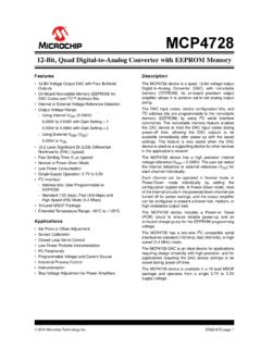
2 24AA64/24LC64 (24XX64*) is a 64 Kbit Electrically Erasable device is organized as eight blocks of 1K x 8-bitmemory with a 2- wire Serial interface. Low voltagedesign permits operation down to with standbyand active currents of only 1 A and 1 mA has been developed for advanced, low power appli-cations such as personal communications or dataacquisition. The 24XX64 also has a page-write capabil-ity for up to 32 bytes of data. Functional address linesallow up to eight devices on the same bus, for up to512 Kbits address space. The 24XX64 is available inthe standard 8-pin PDIP, surface mount SOIC, TSSOPand MSOP TypesBlock DiagramPart NumberVCC RangeMax Clock FrequencyTemp kHz(1) kHzI, ENote 1:100 kHz for VCC < Industrial (I): -40 C to +85 C- Automotive (E):-40 C to +125 C24XX64A0A1A2 Vss12348765 VccWPSCLSDAPDIP/SOIC/TSSOP/MSOP24XX64 XWPVccA0A1 SCLSDAVssA212348765 ROTATED TSSOP(24AA64X/24LC64X)HV GENERATOREEPROM ARRAYPAGE LATCHESYDECXDECSENSE AMPR/W CONTROLI/OCONTROLLOGICI/OMEMORYCONTROLLO GICA0 A1 WPA2 SCLSDAVCCVSS64K I2C Serial EEPROM *24XX64 is used in this document as a generic part number for the 24AA64/24LC64 2 2002 Microchip Technology ELECTRICAL CHARACTERISTICSA bsolute Maximum Ratings inputs and outputs to VCC + temperature.
3 -65 C to +150 CAmbient temp. with power applied ..-40 C to +125 CESD protection on all Characteristics NOTICE: Stresses above those listed under Maximum ratings may cause permanent damage to the is a stress rating only and functional operation of the device at those or any other conditions above thoseindicated in the operational listings of this specification is not implied. Exposure to maximum rating conditionsfor extended periods may affect device CHARACTERISTICSVCC = + to + (I): TAMB = -40 C to +85 CAutomotive (E): TAMB = -40 C to +125 UnitsConditionsD1 VIHWP, SCL and SDA pins D2 High level input voltage VCC V D3 VILLow level input voltage VCCV D4 VHYSH ysteresis of SchmittTrigger VCC V(Note 1)D5 VOLLow level output voltage IOL = mA, VCC = leakage current 10 AVIN =.
4 1V to VCCD7 ILOO utput leakage current 10 AVOUT =.1V to VCCD8 CIN, COUTPin capacitance(all inputs/outputs) 10pF VCC = (Note 1)TAMB = 25 C, FCLK = 1 MHzD9 ICC writeOperating current 3mAVCC = , SCL = 400 kHzD10 ICC read D11 ICCSS tandby current .01 15 A AIndustrialAutomotiveSDA = SCL = VCCWP = VSSNote 1:This parameter is periodically sampled and not 100% :Typical measurements taken at room temperature. 2002 Microchip Technology 324AA64 CharacteristicsAC CHARACTERISTICSVCC = + to + (I):TAMB = -40 C to +85 CAutomotive (E): TAMB = -40 C to +125 UnitsConditions1 FCLKC lock frequency 400100kHz VCC VCC < (24AA64)2 THIGHC lock high time6004000 ns VCC VCC < (24AA64)3 TLOWC lock low time13004700 ns VCC VCC < (24AA64)4 TRSDA and SCL rise time (Note 1) 3001000ns VCC VCC < (24AA64) 5 TFSDA and SCL fall time 300ns(Note 1)6 THD:STASTART condition hold time6004000 ns VCC VCC < (24AA64)7 TSU:STASTART condition setup time6004700 ns VCC VCC < (24AA64)8 THD:DATData input hold time0 ns(Note 2)9 TSU:DATData input setup time100250 ns VCC VCC < (24AA64)10 TSU.
5 STOSTOP condition setup time6004000 ns VCC VCC < (24AA64)11 TAAO utput valid from clock (Note 2) 9003500ns VCC VCC < (24AA64)12 TBUFBus free time: Time the bus must be free before a new transmission can start13004700 ns VCC VCC < (24AA64)13 TOFO utput fall time from VIH min-imum to VIL maximum20+ 250250ns VCC VCC (24AA64)14 TSPI nput filter spike suppression(SDA and SCL pins) 50ns(Notes 1 and 3)15 TWCW rite cycle time (byte or page) 5ms 16 Endurance1M cycles 25 C, VCC = , Block Mode (Note 4)Note 1:Not 100% tested. CB = total capacitance of one bus line in :As a transmitter, the device must provide an internal minimum delay time to bridge the undefined region (minimum 300 ns) of the falling edge of SCL to avoid unintended generation of START or STOP :The combined TSP and VHYS specifications are due to new Schmitt Trigger inputs which provide improved noise spike suppression.
6 This eliminates the need for a TI specification for standard :This parameter is not tested but ensured by characterization. For endurance estimates in a specific appli-cation, please consult the Total Endurance Model which can be obtained on Microchip s website: 4 2002 Microchip Technology 1-1: BUS TIMING DATAFIGURE 1-2: BUS TIMING START/STOP752489101211146 SCLSDAINSDAOUT376D410 STARTSTOPSCLSDA 2002 Microchip Technology 524AA64 FUNCTIONAL DESCRIPTIONThe 24XX64 supports a bi-directional 2- wire bus anddata transmission protocol. A device that sends dataonto the bus is defined as transmitter, and a devicereceiving data as receiver. The bus has to be controlledby a master device which generates the Serial clock(SCL), controls the bus access and generates theSTART and STOP conditions, while the 24XX64 worksas slave.
7 Both master and slave can operate as trans-mitter or receiver, but the master device determineswhich mode is BUS CHARACTERISTICSThe following bus protocol has been defined: Data transfer may be initiated only when the bus is not busy. During data transfer, the data line must remain stable whenever the clock line is HIGH. Changes in the data line while the clock line is HIGH will be interpreted as a START or STOP , the following bus conditions have beendefined (Figure 3-1). Bus not Busy (A)Both data and clock lines remain Start Data Transfer (B)A HIGH to LOW transition of the SDA line while theclock (SCL) is HIGH determines a START condition. Allcommands must be preceded by a START Stop Data Transfer (C)A LOW to HIGH transition of the SDA line while theclock (SCL) is HIGH determines a STOP condition.
8 Alloperations must be ended with a STOP Data Valid (D)The state of the data line represents valid data when,after a START condition, the data line is stable for theduration of the HIGH period of the clock data on the line must be changed during the LOWperiod of the clock signal. There is one clock pulse perbit of data transfer is initiated with a START conditionand terminated with a STOP condition. The number ofthe data bytes transferred between the START andSTOP conditions is determined by the master deviceand is theoretically unlimited, although only the last six-teen will be stored when doing a write operation. Whenan overwrite does occur it will replace data in a first-infirst-out (FIFO) AcknowledgeEach receiving device, when addressed, is obliged togenerate an acknowledge after the reception of eachbyte.
9 The master device must generate an extra clockpulse which is associated with this Acknowledge device that acknowledges, has to pull down theSDA line during the acknowledge clock pulse in such away that the SDA line is stable LOW during the HIGH period of the acknowledge related clock pulse. Ofcourse, setup and hold times must be taken intoaccount. During reads, a master must signal an end ofdata to the slave by not generating an Acknowledge biton the last byte that has been clocked out of the this case, the slave (24XX64) will leave the data lineHIGH to enable the master to generate the STOP 3-1: DATA TRANSFER SEQUENCE ON THE Serial BUSNote:The 24XX64 does not generate anyAcknowledge bits if an internal program-ming cycle is in (A)(B)(D)(D)(A)(C)STARTCONDITIONADDRESS ORACKNOWLEDGEVALIDDATAALLOWEDTO CHANGESTOPCONDITION24AA64/24LC64DS21189F -page 6 2002 Microchip Technology Device Addressing A control byte is the first byte received following theSTART condition from the master device (Figure 3-2).
10 The control byte consists of a four bit control code; forthe 24XX64 this is set as 1010 binary for read and writeoperations. The next three bits of the control byte arethe chip select bits (A2, A1, A0). The chip select bitsallow the use of up to eight 24XX64 devices on thesame bus and are used to select which device isaccessed. The chip select bits in the control byte mustcorrespond to the logic levels on the corresponding A2,A1, and A0 pins for the device to respond. These bitsare in effect the three Most Significant bits of the wordaddress. The last bit of the control byte defines the operation tobe performed. When set to a one a read operation isselected, and when set to a zero a write operation isselected. The next two bytes received define theaddress of the first data byte (Figure 3-3).