Transcription of 28-Pin, Low-Power, High-Performance …
1 2017 Microchip Technology 1 PIC18(L)F25/26K83 DescriptionThe PIC18(L)FXXK83 is a full-featured CAN product family that can be used in automotive and industrial multitude of communication peripherals found on the product family, such as CAN, SPI, two I2Cs, two UARTs, LIN,DMX, and DALI can handle a wide range of wired and wireless (using external modules) communication protocols forintelligent applications. This family includes a 12-bit ADC with Computation (ADC2) extensions for automated signalanalysis to reduce the complexity of the application. This, combined with the Core Independent Peripherals integrationcapabilities, enables functions for motor control, power supply, sensor, signal and user interface Features C Compiler Optimized RISC Architecture Operating Speed:- Up to 64 MHz clock operation- ns minimum instruction cycle Two Direct Memory Access (DMA) Controllers:- Data transfers to SFR/GPR spaces from either Program Flash Memory, Data EEPROM or SFR/GPR spaces- User-programmable source and destination sizes- Hardware and software-triggered data transfers System Bus Arbiter with User-Configurable Priorities for Scanner and DMA1/DMA2 with respect to the main line and interrupt execution Vectored Interrupt Capability.
2 - Selectable high /low priority- Fixed interrupt latency- Programmable vector table base address 31-Level Deep Hardware Stack Low-Current power -on Reset (POR) Configurable power -up Timer (PWRT) Brown-Out Reset (BOR) Low- power BOR (LPBOR) Option Windowed Watchdog Timer (WWDT):- Variable prescaler selection- Variable window size selection- Configurable in hardware or softwareMemory Up to 64 KB Flash Program Memory Up to 4 KB Data SRAM Memory Up to 1 KB Data EEPROM Memory Access Partition (MAP):- Configurable boot and app region sizes with individual write-protections Programmable Code Protection Device Information Area (DIA) stores:- Unique IDs and Device IDs- Temp Sensor factory-calibrated data- Fixed Voltage Reference calibrated data Device Configuration Information (DCI) stores:- Erase row size- Number of write latches per row- Number of user rows- Data EEPROM memory size- Pin countOperating Characteristics Operating Voltage Range:- to (PIC18LF25/26K83)- to (PIC18F25/26K83) Temperature Range:- Industrial: -40 C to 85 C- Extended: -40 C to 125 CPower-Saving Functionality DOZE mode: Ability to run CPU core slower than the system clock IDLE mode: Ability to halt CPU core while internal peripherals continue operating SLEEP mode: Lowest power consumption Peripheral Module Disable (PMD): -Ability to disable unused peripherals to minimize power consumption28-Pin, Low- power , High-Performance Microcontrollers with CAN Technology 2017 Microchip Technology 2 PIC18(L)F25/26K83eXtreme Low- power (XLP) Features Sleep mode: 60 nA @ , typical Windowed Watchdog Timer: 720 nA @ , typical Secondary Oscillator: 580 nA @ 32 kHz Operating Current.
3 - 4 uA @ 32 kHz, , typical - 45 uA/MHz @ , typicalDigital Peripherals Three 8-Bit Timers (TMR2/4/6) with Hardware Limit Timer (HLT):- Hardware monitoring and Fault detection Four 16-Bit Timers (TMR0/1/3/5) Four Configurable Logic Cell (CLC): - Integrated combinational and sequential logic Three Complementary Waveform Generators (CWGs):- Rising and falling edge dead-band control- Full-bridge, half-bridge, 1-channel drive- Multiple signal sources- Programmable dead band- Fault-shutdown input Four Capture/Compare/PWM (CCP) modules Four 10-bit Pulse-Width Modulators (PWMs) Numerically Controlled Oscillator (NCO):- Generates true linear frequency control- high resolution using 20-bit accumulator and 20-bit increment values DSM: Data Signal Modulator:- Multiplex two carrier clocks, with glitch pre-vention feature- Multiple sources for each carrier Programmable CRC with Memory Scan:- Reliable data/program memory monitoring for fail-safe operation ( , Class B)- Calculate CRC over any portion of program memory Two UART Modules:- Modules are Asynchronous, RS-232, RS-485 compatibility.
4 - One of the UART modules supports LIN Master and Slave, DMX mode, DALI Gear and Device protocols- Automatic and user-timed BREAK period generation- DMA Compatible- Automatic checksums- Programmable 1, , and two Stop bits- Wake-up on BREAK reception One SPI module:- Configurable length bytes- Configurable length data packets- Receive-without-transmit option- Transmit-without-receive option- Transfer byte counter- Separate Transmit and Receive Buffers with 2-byte FIFO and DMA capabilities CAN module:- Conforms to CAN Active Specification- Three operating modes: Legacy (compatible with existing PIC18 CXX8/FXX8 CAN modules), Enhanced mode, and FIFO Message bit rates up to 1 Mbps- DeviceNet data byte filter support- Six programmable receive/transmit buffers- Three dedicated transmit buffers- Two dedicated receive buffers- 16 Full, 29-bit acceptance filters with dynamic association- Three full, 29-bit acceptance masks- Automatic remote frame handling- Advanced error management features.
5 Two I2C modules, SMBus, PMBus compatible:- Dedicated Address, Transmit and Receive buffers- Bus Collision Detection with arbitration- Bus time-out detection and handling- Multi-Master mode- Separate Transmit and Receive Buffers with 2-byte FIFO and DMA capabilities-I2C, SMBus and SMBus , and input level selections Device I/O Port Features:- 25 I/O pins (PIC18(L)F25K83)- One input-only pin- Individually programmable I/O direction, open-drain, slew rate, weak pull-up control- Interrupt-on-change- Three External Interrupt Pins Peripheral Pin Select (PPS):- Enables pin mapping of digital I/O Two Signal Measurement Timer (SMT):- 24-bit timer/counter with prescaler 2017 Microchip Technology 3 PIC18(L)F25/26K83 Analog Peripherals Analog-to-Digital Converter with Computation (ADC2): - 12-bit with up to 24 external channels - Automated post-processing- Automated math functions on input signals: averaging, filter calculations, oversampling and threshold comparison - Operates in Sleep- Integrated charge pump for improved low-voltage operation Hardware Capacitive Voltage Divider (CVD):- Automates touch sampling and reduces soft-ware size and CPU usage when touch or proximity sensing is required- Adjustable sample and hold capacitor array- Two guard ring output drives Temperature Sensor:- Internal connection to ADC- Can be calibrated for improved accuracy Two Comparators:- Low- power / high -Speed mode - Fixed Voltage Reference at noninverting input(s) - Comparator outputs externally accessible 5-Bit Digital-to-Analog Converter (DAC).
6 - 5-bit resolution, rail-to-rail- Positive Reference Selection - Unbuffered I/O pin output- Internal connections to ADCs and comparators Voltage Reference:- Fixed Voltage Reference with , and output levelsFlexible Oscillator Structure high -Precision Internal Oscillator:- Selectable frequency range up to 64 MHz- 1% at calibration (nominal) Low- power Internal 32 kHz Oscillator(LFINTOSC) External 32 kHz Crystal Oscillator (SOCS) External Oscillator Block with:- x4 PLL with external sources- Three crystal/resonator modes up to 20 MHz- Three external clock modes up to 20 MHz Fail-Safe Clock Monitor Oscillator Start-up Timer (OST):- Ensures stability of crystal oscillator sources 2017 Microchip Technology 4 PIC18(L)F25/26K83 TABLE 1:PIC18(L)FXXK83 FAMILY TYPESD eviceData Sheet IndexProgram Flash Memory (KB)Data EEPROM (B)Data SRAM (bytes)I/O Pins12-bit ADC2 (ch)5-bit DACC omparator8-bit/ (with HLT)/16-bit TimerWindow Watchdog Timer (WWDT)Signal Measurement Timer (SMT)CCP/10-bit PWMCWGNCOCLCZero-Cross DetectDirect Memory Access (DMA)Memory Access PartitionVectored InterruptsCANUART with ProtocolsI2C/SPIP eripheral Pin SelectPeripheral Module DisableDebug(1)PIC18(L)F25K83(A)32102420 482524123/3YY4/4114Y2 YYY21/1 YYIPIC18(L)F26K83(A)64102440962524123/3Y Y4/4114Y2 YYY21/1 YYINote1:I - Debugging integrated on Sheet Index: A:DS40001943 PIC18(L)F25/26K83 Data Sheet, 28-PinNote:For other small form-factor package availability and marking information, or contact your local sales office.
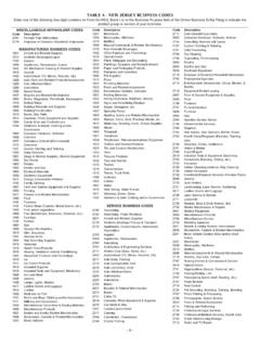
7 2017 Microchip Technology 5 PIC18(L)F25/26K83 Pin DiagramsTABLE 2:PACKAGESD eviceSPDIPSOICSSOPUQFNQFNPIC18(L)F25K83 PIC18(L)F26K83 Note 1:Pin details are subject to (L)F25K8312345678910 VPP/MCLR/RE3RA0RA1RA2RA3RA4RA5RB6/ICSPCL KRB5RB4RB3RB2RB1RB0 VDDVSS1112131415161718192028272625242322 21 VSSRA7RA6RC0RC1RC2RC3RC5RC4RC7RC6RB7/ICS PDATNote:See Ta b l e 3 for location of all peripheral SPDIP, SOIC, SSOP2361181920211571617RC054RB7/ICSPDATR B6/ICSPCLKRB5RB4RB0 VDDVSSRC7RC6RC5RC4RE3/MCLR/VPPRA0RA1RA2R A3RA4RA5 VSSRA7RA6RC1RC2RC391013814121127 262328222425RB3RB2RB1 PIC18(L)F26K83 Note 1:See Ta b l e 3 for location of all peripheral :It is recommended that the exposed bottom pad be connected to VSS, however it must not be theonly VSS connection to the QFN ( ), UQFN ( ) 2017 Microchip Technology 6 PIC18(L)F25/26K83 Pin Allocation TablesTABLE 3:28-PIN ALLOCATION TABLE (PIC18(L)F25/26K83)I/O28-Pin SPDIP/SOIC/SSOP28-Pin (U)QFNADCV oltage ReferenceDACC omparatorsZero Cross DetectI2 CSPIUARTDSMT imers/SMTCCP and PWMCWGCLCNCOC lock Reference (CLKR)ECANI nterrupt-on ChangeBasicRA0227 ANA0 C1IN0-C2IN0- CLCIN0(1) IOCA0 RA1328 ANA1 C1IN1-C2IN1- CLCIN1(1) IOCA1 RA241 ANA2 VREF-DAC1 OUT1C1IN0+C2IN0+ IOCA2 RA352 ANA3 VREF+ C1IN1+ MD1 CARL(1) IOCA3 RA463 ANA4 MD1 CARH(1)T0 CKI(1) IOCA4 RA574 ANA5 SS1(1,3) MD1 SRC(1) IOCA5 RA6107 ANA6 IOCA6 OSC2 CLKOUTRA796 ANA7 IOCA7 OSC1 CLKINRB02118 ANB0 C2IN1+ZCD CCP4(1)CWG1(1) IOCB0 INT0(1) RB12219 ANB1 C1IN3-C2IN3- SCL2(1,3,4) CWG2(1) IOCB1 INT1(1) RB22320 ANB2 SDA2(1,3,4) CWG3(1) IOCB2 INT2(1) RB32421 ANB3 C1IN2-C2IN2- CANRX(1)IOCB3 RB42522 ANB4 ADACT(1) T5G(1)SMT2 WIN(1) CLCIN2(1)
8 IOCB4 RB52623 ANB5 T1G(1)SMT2 SIG(1)CCP3(1) CLCIN3(1) IOCB5 RB62724 ANB6 CTS2(1) IOCB6 ICSPCLKRB72825 ANB7 DAC1 OUT2 RX2(1) T6IN(1) IOCB7 ICSPDATRC0118 ANC0 T1 CKI(1)T3 CKI(1)T3G(1)SMT1 WIN(1) IOCC0 SOSCORC1129 ANC1 SMT1 SIG(1)CCP2(1) IOCC1 SOSCIRC21310 ANC2 T5 CKI(1)CCP1(1) IOCC2 RC31411 ANC3 SCL1(1)SCK1(1,3) T2IN(1) IOCC3 Note1:This is a PPS remappable input signal. The input function may be moved from the default location shown to one of several other PORTx :All output signals shown in this row are PPS :This is a bidirectional signal. For normal module operation, the firmware should map this signal to the same pin in both the PPS input and PPS output :These pins can be configured for I2C and SMBTM logic levels; the SCLx/SDAx signals may be assigned to any of the RB1/RB2/RC3/RC4 pins. PPS assignments to the other pins ( , RA5) will operate, but input logic levels will be standard TTL/ST as selected by the INLVL register, instead of the I2C specific or SMBUS input buffer thresholds.
9 2017 Microchip Technology 7 PIC18(L)F25/26K83RC41512 ANC4 SDA1(1)SDI1(1) IOCC4 RC51613 ANC5 T4IN(1) IOCC5 RC61714 ANC6 CTS1(1) IOCC6 RC71815 ANC7 RX1(1) IOCC7 RE3126 IOCE3 MCLRVPPVDD2017 VSS8,195,16 OUT(2) ADGRDAADGRDB C1 OUTC2 OUT SDA1 SCL1 SDA2 SCL2SS1 SCK1 SDO1 DTR1 RTS1TX1 DTR2 RTS2TX2 DSMTMR0 CCP1 CCP2 CCP3 CCP4 PWM5 OUTPWM6 OUTPWM7 OUTPWM8 OUTCWG1 ACWG1 BCWG1 CCWG1 DCWG2 ACWG2 BCWG2 CCWG2 DCWG3 ACWG3 BCWG3 CCWG3 DCLC1 OUTCLC2 OUTCLC3 OUTCLC4 OUTNCOCLKRCANTX TABLE 3:28-PIN ALLOCATION TABLE (PIC18(L)F25/26K83) (CONTINUED)I/O28-Pin SPDIP/SOIC/SSOP28-Pin (U)QFNADCV oltage ReferenceDACC omparatorsZero Cross DetectI2 CSPIUARTDSMT imers/SMTCCP and PWMCWGCLCNCOC lock Reference (CLKR)ECANI nterrupt-on ChangeBasicNote1:This is a PPS remappable input signal. The input function may be moved from the default location shown to one of several other PORTx :All output signals shown in this row are PPS :This is a bidirectional signal.
10 For normal module operation, the firmware should map this signal to the same pin in both the PPS input and PPS output :These pins can be configured for I2C and SMBTM logic levels; the SCLx/SDAx signals may be assigned to any of the RB1/RB2/RC3/RC4 pins. PPS assignments to the other pins ( , RA5) will operate, but input logic levels will be standard TTL/ST as selected by the INLVL register, instead of the I2C specific or SMBUS input buffer thresholds. 2017 Microchip Technology 8 PIC18(L)F25/26K83 Table of Overview .. for Getting Started with PIC18(L)F25/26K83 Microcontrollers .. Organization .. Configuration .. Module (with Fail-Safe Clock Monitor) .. Clock Output Module .. Controller .. power -Saving Operation Modes .. Windowed Watchdog Timer (WWDT) .. 8x8 Hardware Nonvolatile Memory (NVM) Cyclic Redundancy Check (CRC) Module with Memory Direct Memory Access (DMA).