Transcription of 2A, 600V N-CHANNEL POWER MOSFET - Unisonic
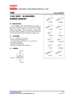
1 Unisonic TECHNOLOGIES CO., LTD 2n60l POWER MOSFET 1 of 7 Copyright 2014 Unisonic Technologies Co., Ltd 2A, 600V N-CHANNEL POWER MOSFET DESCRIPTION The UTC 2n60l is a high voltage MOSFET and is designed to have better characteristics, such as fast switching time, low gate charge, low on-state resistance and have a high rugged avalanche characteristics. This POWER MOSFET is usually used at high speed switching applications in POWER supplies, PWM motor controls, high efficient DC to DC converters and bridge circuits. FEATURES * RDS(ON) < 5 @ VGS = 10V, ID =1A * Fast switching capability * Avalanche energy specified * Improved dv/dt capability, high ruggedness SYMBOL 2n60l POWER MOSFET Unisonic TECHNOLOGIES CO., LTD 2 of 7 ORDERING INFORMATION Ordering Number Package Pin Assignment Packing Lead Free Halogen Free 1 2 3 2N60LL-TA3-T 2N60LG-TA3-T TO-220 G D S Tube 2N60LL-TF1-T 2N60LG-TF1-T TO-220F1G D S Tube 2N60LL-TF2-T 2N60LG-TF2-T TO-220F2G D S Tube 2N60LL-TF3-T 2N60LG-TF3-T TO-220F G D S Tube
2 2N60LL-TF3T-T 2N60LG-TF3T-T TO-220F3G D S Tube 2N60LL-TM3-T 2N60LG-TM3-T TO-251 G D S Tube 2N60LL-TMA-T 2N60LG-TMA-T TO-251L G D S Tube 2N60LL-TMS-T 2N60LG-TMS-T TO-251S G D S Tube 2N60LL-TMS2-T 2N60LG-TMS2-T TO-251S2G D S Tube 2N60LL-TMS4-T 2N60LG-TMS4-T TO-251S4G D S Tube 2N60LL-TN3-R 2N60LG-TN3-R TO-252 G D S Tape Reel 2N60LL-TND-R 2N60LG-TND-R TO-252D G D S Tape Reel 2N60LL-T2Q-T 2N60LG-T2Q-T TO-262 G D S Tube 2N60LL -T60-K 2N60LG-T60-K TO-126 G D S Bulk Note: Pin Assignment: G: Gate D: Drain S.
3 Source MARKING PACKAGE MARKING TO-220 TO-220F TO-220F1 TO-220F2 TO-220F3 TO-251 TO-251L TO-251S TO-251S2 TO-251S4 TO-252 TO-252D TO-262 TO-126 2n60l POWER MOSFET Unisonic TECHNOLOGIES CO., LTD 3 of 7 ABSOLUTE MAXIMUM RATINGS (TC = 25 С, unless otherwise specified) PARAMETER SYMBOL RATINGS UNIT Drain-Source Voltage VDSS 600 V Gate-Source Voltage VGSS 30 V Avalanche Current (Note 2)
4 IAR A Drain Current Continuous ID A Pulsed (Note 2) IDM A Avalanche Energy Single Pulsed (Note 3)EAS 140 mJ Repetitive (Note 2) EAR mJ Peak Diode Recovery dv/dt (Note 4) dv/dt V/ns POWER Dissipation TO-220/TO-262 PD 54 W TO-220F/TO-220F1 TO-220F3 23 W TO-220F2 25 W TO-251/TO-251L TO-251S/TO-251S2 TO-251S4/TO-252 TO-252D 44 W TO-126 W Junction Temperature TJ +150 С
5 Ambient Operating Temperature TOPR -55 ~ +150 С Storage Temperature TSTG -55 ~ +150 С Notes: 1. Absolute maximum ratings are those values beyond which the device could be permanently damaged. Absolute maximum ratings are stress ratings only and functional device operation is not implied. 2. Repetitive Rating : Pulse width limited by TJ 3. L=64mH, IAS= , VDD=50V, RG=25 , Starting TJ = 25 C 4. ISD , di/dt 200A/ s, VDD BVDSS, Starting TJ = 25 C THERMAL DATA PARAMETER PACKAGE SYMBOL RATINGS UNIT Junction to Ambient TO-220/TO-220F TO-220F1/TO-220F2 TO-220F3/TO-262 JA С/W TO-251/TO-251L TO-251S/TO-251S2 TO-251S4/TO-252 TO-252D 100 С/W TO-126 132 С/W Junction to Case TO-220/TO-262 JC С/W TO-220F/TO-220F1 TO-220F3 С/W TO-220F2 5 С/W TO-251/TO-251L TO-251S/TO-251S2 TO-251S4/TO-252 TO-252D
6 С/W TO-126 10 С/W 2n60l POWER MOSFET Unisonic TECHNOLOGIES CO., LTD 4 of 7 ELECTRICAL CHARACTERISTICS (TJ =25 С, unless otherwise specified) PARAMETER SYMBOL TEST CONDITIONS MIN TYP MAX UNITOFF CHARACTERISTICS Drain-Source Breakdown Voltage BVDSS VGS = 0V, ID = 250 A 600 V Drain-Source Leakage Current IDSS VDS = 600V, VGS = 0V 10 AGate-Source Leakage Current Forward IGSS VGS = 30V, VDS = 0V 100nAReverse VGS = -30V, VDS = 0V -100nABreakdown Voltage Temperature Coefficient BVDSS /TJID=250 A, Referenced to 25 C V/ СON CHARACTERISTICS Gate Threshold Voltage VGS(TH)
7 VDS = VGS, ID = 250 A Static Drain-Source On-State Resistance RDS(ON) VGS = 10V, ID =1A DYNAMIC CHARACTERISTICS Input Capacitance CISS VDS =25V, VGS =0V, f =1 MHz 300 350pFOutput Capacitance COSS 30 50pFReverse Transfer Capacitance CRSS 7 10pFSWITCHING CHARACTERISTICS Turn-On Delay Time tD(ON) VDD =300V, ID = , RG=25 (Note 1, 2) 30 60nsTurn-On Rise Time tR 25 60nsTurn-Off Delay Time tD(OFF) 70 90nsTurn-Off Fall Time tF 30 60nsTotal Gate Charge QG VDS=480V, VGS=10V, ID= (Note 1, 2)
8 30 40nCGate-Source Charge QGS 8 nCGate-Drain Charge QGD 10 nCDRAIN-SOURCE DIODE CHARACTERISTICS Drain-Source Diode Forward Voltage VSD VGS = 0 V, ISD = A Continuous Drain-Source Current ISD Pulsed Drain-Source Current ISM Reverse Recovery Time tRR VGS = 0 V, ISD = , di/dt = 100 A/ s (Note1) 180 nsReverse Recovery Charge QRR CNotes: 1.
9 Pulse Test: Pulse width 300 s, Duty cycle 2%. 2. Essentially independent of operating temperature. 2n60l POWER MOSFET Unisonic TECHNOLOGIES CO., LTD 5 of 7 TEST CIRCUITS AND WAVEFORMS Same Type as +* dv/dt controlled by RG* ISD controlled by pulse period* Under Test-+ Peak Diode Recovery dv/dt Test Circuit P. (Driver)ISD( )IFM, Body Diode Forward Currentdi/dtIRMBody Diode Reverse CurrentBody Diode Recovery dv/dtBody Diode Forward Voltage DropVDD10 VVDS( )VGS= Peak Diode Recovery dv/dt Waveforms 2n60l POWER MOSFET Unisonic TECHNOLOGIES CO., LTD 6 of 7 TEST CIRCUITS AND WAVEFORMS (Cont.) VDS90%10%VGStD(ON)tRtD(OFF)tFSwitching Test Circuit Switching Waveforms 10 VChargeQGSQGDQGVGSGate Charge Test Circuit Gate Charge Waveform VDDtpTimeBVDSSIASID(t)VDS(t) Unclamped Inductive Switching Test Circuit Unclamped Inductive Switching Waveforms 2n60l POWER MOSFET Unisonic TECHNOLOGIES CO.
10 , LTD 7 of 7 TYPICAL CHARACTERISTICS Drain Current vs. Drain-Source Breakdown VoltageDrain Current, ID( A)Drain-Source Breakdown Voltage, BVDSS(V)10 Drain Current vs. Gate Threshold VoltageDrain Current, ID( A)Gate Threshold Voltage, VTH (V)2354050100150200250300020060080010005 0100150200250300400 Drain-Source On-State ResistanceCharacteristicsDrain Current, ID(A)Drain to Source Voltage, VDS(V) 4 6 Drain-Soarce Current vs. Source to Drain VoltageSource to Drain Voltage, VSD (V)Coutinuous Drain-Soarce Current, ISD (A) , ID=1A UTC assumes no responsibility for equipment failures that result from using products at values thatexceed, even momentarily, rated values (such as maximum ratings, operating condition ranges, orother parameters) listed in products specifications of any and all UTC products described or containedherein.