Transcription of AL8860 40V 1.5A BUCK LED DRIVER Description Pin …
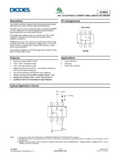
1 AL8860 Document number: DS39014 Rev. 4 - 2 1 of 17 July 2018 Diodes Incorporated AL8860 40V buck LED DRIVER Description The AL8860 is a hysteresis mode DC/DC step-down converter, designed for driving single or multiple series connected LEDs efficiently from a voltage source higher than the LED voltage. The device can operate from an input supply between and 40V and provide an externally adjustable output current up to 1A for TSOT25 package and for MSOP-8EP package. Depending upon supply voltage and external components, this converter can provide up to 40 watts output power. The AL8860 integrates the power switch and a high-side output current sensing circuit, which uses an external resistor to set the nominal average output current.
2 Dimming can be realized by applying an external control signal to the CTRL pin. The CTRL pin will accept either a DC voltage signal or a PWM signal. The soft-start time can be adjusted by an external capacitor from the CTRL pin to ground. Applying a voltage of or lower to the CTRL pin can turn off the output and make the device enter into standby state with low current consumption. Features Low BOM Counts Wide Input Voltage Range: to 40V Output Current Up to Internal 40V NDMOS Switch Typical 5% Output Current Accuracy Single Pin for On/Off and Brightness Control by DC Voltage or PWM Signal Recommended Analog Dimming Range: 5% ~100% Soft-Start High Efficiency (Up to 97%) LED Short Protection Inherent Open-Circuit LED Protection Over Temperature Protection (OTP) Up to 1 MHz Switching Frequency Pb-Free TSOT25 and MSOP-8EP Packages Totally Lead-Free & Fully RoHS Compliant (Notes 1 & 2) Halogen and Antimony Free.
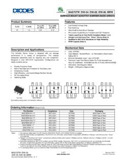
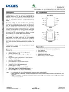
3 Green Device (Note 3) Pin Assignments (Top View) TSOT25 (Top View) MSOP-8EP Applications LED Retrofit for Low Voltage Halogen Low Voltage Industrial Lighting Illuminated Signs External DRIVER with Multiple Channels Notes: 1. No purposely added lead. Fully EU Directive 2002/95/EC (RoHS), 2011/65/EU (RoHS 2) & 2015/863/EU (RoHS 3) compliant. 2. See for more information about Diodes Incorporated s definitions of Halogen- and Antimony-free, "Green" and Lead-free. 3. Halogen- and Antimony-free "Green products are defined as those which contain <900ppm bromine, <900ppm chlorine (<1500ppm total Br + Cl) and <1000ppm antimony compounds.
4 EP AL8860 Document number: DS39014 Rev. 4 - 2 2 of 17 July 2018 Diodes Incorporated AL8860 Typical Applications Circuit Pin descriptions Pin Number Pin Name Function TSOT25 MSOP-8EP 1 5,6 SW Drain of NDMOS switch. 2 2,3 GND Ground (0V) 3 4 CTRL Multi-function On/Off and brightness control pin: Leave floating for normal operation. Drive to voltage below to turn off output current Drive with DC voltage ( < CTRL< ) to adjust output current from 0 to 100% of IOUT_NOM Drive with PWM signal from open-collector or open-drain transistor, to adjust output current. Linear adjustment range from 1% to 100% of IOUT_NOM for f < 500Hz Connect a capacitor from this pin to ground to increase soft-start time.
5 (Default soft-start time = Additional soft-start time is ) 4 1 SET Connect resistor RS from this pin to VIN to define nominal average output current: IOUT_NOM = 5 8 VIN Input voltage ( to 40V). Decouple to ground with 10 F or higher X7R ceramic capacitor close to device. - EP EP Exposed pad. Connect to GND and thermal mass for enhanced thermal impedance. Should not be used as electrical ground conduction path. - 7 N/C No Connection Functional Block Diagram VDD GeneratorBG & ReferencePWM/DC DimmingCurrent MonitorHysteresis ControlOTPL ogic & (8)3(4)2(2,3)1(5,6)4(1) A B A for TSOT25 B for MSOP-8EP AL8860 Document number: DS39014 Rev. 4 - 2 3 of 17 July 2018 Diodes Incorporated AL8860 Absolute Maximum Ratings (@TA = +25 C, unless otherwise specified) (Note 4) Symbol Parameter Rating Unit ESD HBM Human Body Model ESD Protection kV ESD MM Machine Model ESD Protection 200 V VIN Input Voltage to +42 V VSW, VSET SW, SET Pin Voltage to +42 V VCTRL CTRL Pin Voltage to +6 V TJ Operating Junction Temperature +150 C TSTG Storage Temperature Range -65 to +150 C TLEAD Lead Temperature (Soldering, 10s) +260 C JA Thermal Resistance (Junction to Ambient) TSOT25 (Note 5) 147 C/W MSOP-8EP (Note 6) 56 JC Thermal Resistance (Junction to Case) TSOT25 (Note 5) 27 C/W MSOP-8EP (Note 6) 15 Note: 4.
6 Stresses greater than those listed under Absolute Maximum Ratings may cause permanent damage to the device. These are stress ratings only, and functional operation of the device at these or any other conditions beyond those indicated under Recommended Operating Conditions is not implied. Exposure to Absolute Maximum Ratings for extended periods may affect device reliability. 5. Device mounted on 1"x1" FR-4 MRP substrate PC board, 2oz cooper, with minimum recommended pad layout. 6. Device mounted on 2"*2" FR-4 substrate PC board, 2oz copper, with minimum recommended pad layout. Recommended Operating Conditions (@TA = +25 C, unless otherwise specified.) Symbol Parameter Min Max Unit VIN Input Voltage 40 V fSW Switching Frequency - 1 MHz IOUT Continuous Output Current TSOT25 - 1 A MSOP-8EP - - Recommended Analog Dimming Range 5 100 % TA Operating Ambient Temperature -40 +85 C TJ Operating Junction Temperature -40 +125 C AL8860 Document number: DS39014 Rev.
7 4 - 2 4 of 17 July 2018 Diodes Incorporated AL8860 Electrical Characteristics (@TA = +25 C, unless otherwise specified.) Symbol Parameter Condition Min Typ Max Unit VIN Input Voltage - - 40 V IQ Quiescent Current CTRL Pin Floating, VIN =16V - - mA ISHDN Shutdown Supply Current CTRL Pin Grounded - 50 80 A VSENSE Mean Current Sense Threshold Voltage Measured on SET Pin with Respect to VIN 96 100 104 mV VSENSE_HYS Sense Threshold Hysteresis - - 20 - % ISET SET Pin Input Current VSET = VIN - 8 - A VEN CTRL Range on CTRL Pin For Analog Dimming - V VEN(ON) DC Voltage on CTRL Pin to Enable VEN Rising - - V VEN(OFF) DC Voltage on CTRL Pin to Disable VEN Falling - - V RSW SW Switch On Resistance @ISW = 100mA - - ISW(LEAK)
8 SW Switch Leakage Current - - - 5 A tSS Soft Start Time VIN = 16V, CEN = 1nF - - ms fSW Operating Frequency VIN = 16V, VO = (3 LEDs) L = 47 F, I = (ILED = 1A) - 250 - kHz tON_REC Recommended Minimum Switch ON Time For 4% Accuracy - 500 - ns fSW(MAX) Recommended Maximum Switch Frequency - - - MHz DSW(MAX) Max Duty Cycle - - 98 - % DSW Recommended Duty Cycle Range - 25 - 75 % tPD Internal Comparator Propagation Delay (Note 7) - - 45 - ns TOTP Over Temperature Protection - - +150 - C TOTP_HYS Temperature Protection Hysteresis - - +30 - C Note: 7. Guaranteed by design. AL8860 Document number: DS39014 Rev. 4 - 2 5 of 17 July 2018 Diodes Incorporated AL8860 Typical Performance Characteristics (@TA = +25 C, VIN = 16V, unless otherwise specified.)
9 Quiescent Current vs. Input Voltage Quiescent Current vs. Temperature Shutdown Current vs. Input voltage Shutdown Current vs. Temperature SET Threshold Voltage vs. Input voltage PWM Dimming (VIN=16V, 3 LEDs, 47 H, Rs= ) Output Current vs. Duty Cycle 4681012141618202224262830323436384036038 0400420440460480500520540560 Quiescent Current ( A)Input Voltage(V)468101214161820222426283032343 638404042444648505254565860 Shutdown Current ( A)Input Voltage(V)468101214161820222426283032343 638406065707580859095100105110115120 SET threshold Voltage(mV)Input Voltage(V) VTH_H VTH_mean VTH_L-50-2502550751001254004204404604805 00520540560580600 Quiescent Current ( A)Temperature('C) VIN=16V-50-25025507510012501020304050607 08090100 Shutdown Current ( A)Temperature('C)
10 VIN=16V010203040506070809010002040608010 0120140160180200220240260280300320340 Output Current (mA)Duty Cycle(%)L=47 H,freq=680kHz fPWM=100Hz fPWM=200Hz fPWM=500Hz fPWM=1kHz AL8860 Document number: DS39014 Rev. 4 - 2 6 of 17 July 2018 Diodes Incorporated AL8860 Typical Performance Characteristics (Cont.) (@TA = +25 C, VIN = 16V, unless otherwise specified.) Analog Dimming (VIN=16V, 3 LEDs, 47 H, Rs= ) Efficiency vs. Input Voltage LED Current vs. CTRL Pin Voltage (TSOT25, Rs= , L=100 H) Efficiency vs. Input Voltage Efficiency vs.
