Transcription of AN ASYMMETRICAL INTERLEAVED DC-DC BOOST …
1 International Journal of Technology and Engineering System (IJTES) Vol 6. Jan-March 2014 Pp. 157-161 gopalax Journals, Singapore available at : ISSN: 0976-1345 gopalax Publications 157 AN ASYMMETRICAL INTERLEAVED DC-DC BOOST CONVERTER FOR HIGH STEP UP APPLICATIONS , PG Scholar, Karpaga Vinayaga College of Engineering & Technology, Chennai, India1 Assistant Professor, Karpaga Vinayaga College of Engineering & Technology, Chennai, India2 ABSTRACT A new high step-up converter is projected for a photovoltaic system. An ASYMMETRICAL INTERLEAVED high step-up converter achieves high step up gain through a voltage multiplier module. The voltage multiplier module is organised by a conventional BOOST converter and coupled inductors.
2 A conventional BOOST converter is incorporated to achieve a considerably higher voltage conversion ratio. This configuration reduces the current stress through each power switch. And also constrains the input current ripple, which decreases the conduction losses of MOSFETs. Since the energy stored in leakage inductances is recycled to the output terminal, the efficiency of the system is improved. Keywords: ASYMMETRICAL INTERLEAVED Converter, Coupled Inductor, PV system I. INTRODUCTION Mounting energy shortage has valued the use of renewable energy systems like PV system. But the energy obtained from renewable systems is considerably low. Thus, high step-up DC-DC converters are widely engaged in many renewable energy applications [7].
3 Photovoltaic systems are predicted to play an important role in future energy creation [12]. These systems convert light energy into electrical energy, and by using step-up converter they transfer low voltage into high voltage. II. CONVENTIONAL ASYMMETRICAL INTERLEAVED CONVERTER An ASYMMETRICAL INTERLEAVED converter is extensively used for achieving high step-up conversion and for high-power application [14]. A conventional BOOST converter and two coupled inductors are located in the voltage multiplier module, which is mounted on a BOOST converter to form an ASYMMETRICAL INTERLEAVED structure. Primary windings of the coupled inductors are engaged to reduce the input current ripple, and secondary windings of the coupled inductors are connected in series to lengthen the voltage gain.
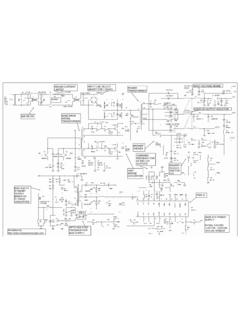
4 Circuit diagram of proposed system The proposed converter operates in continuous conduction mode (CCM). The duty cycles during steady operation are INTERLEAVED with a 180 phase shift and it is greater than III. MODES OF OPERATION Mode 1 [t0, t1]: At t=t0, The power switches S1 and S2 are turned ON. Now all the diodes are reversed-biased and the Magnetizing inductors Lm1 and Lm2 as well as leakage inductors Lk1 and Lk2 are linearly charged by the input voltage source Vin. Mode 2 [t1, t2]: At t=t1, the power switch S2 is turned OFF, therefore the diodes D2 and D4 are turned ON. The energy stored in the magnetizing inductor Lm2 is transferred to the secondary side and it charges the output filter capacitor C3.
5 The input voltage source, and the energy stored in magnetizing inductor Lm2, leakage inductor Lk2, International Journal of Technology and Engineering System (IJTES) Vol 6. Jan-March 2014 Pp. 157-161 gopalax Journals, Singapore available at : ISSN: 0976-1345 gopalax Publications 158 voltage-lift capacitor Cb is discharged to the output filter capacitor C1 through the diode D2, thereby extending the voltage on C1 . Mode 3 [t2, t3]: At t=t2, the diode D2 automatically turns OFF because the overall energy stored in the leakage inductor Lk2 is entirely released to the output filter capacitor C1. The Magnetizing inductor Lm2 transfers energy to the secondary side and it charges the output filter capacitor C3 through the diode D4 until t3.
6 Mode 4 [t3, t4]: At t=t3, the power switch S2 is turned ON and all the diodes are turned OFF. Now all the diodes are reversed-biased and the Magnetizing inductors Lm1 and Lm2 as well as leakage inductors Lk1 and Lk2 are linearly charged by the input voltage source Vin. Mode 5 [t4, t5]: At t=t4, the power switch S1 is turned OFF, therefore diodes D1 and D3 are turned ON. Now the energy stored in the magnetizing inductor Lm1 is transferred to the secondary side and it charges the output filter capacitor C2. The input voltage source and the energy stored in the magnetizing inductor Lm1 is completely released to the voltage-lift capacitor Cb through the diode D1, which supplies extra energy to Cb.
7 Mode 6 [t5, t0]: At t=t5, the diode D1 is automatically turns OFF because the entire energy stored in the leakage inductor Lk1 is totally released to voltage-lift capacitor Cb. Now the magnetizing inductor Lm1 transfers energy to the secondary side and it charges the output filter capacitor C2 through the diode D3 until t0. Modes of operation of the proposed system IV. Voltage Gain From the equivalent circuit of the proposed converter, the first phase converter is considered as a conventional BOOST converter. Thus the voltage derived from VCb can be expressed as, = (1) When the power switch S1 is switched ON and the power switch S2 is turned OFF, the voltage VC1 can be derived from, = + = (2) Steady Waveform of the Proposed Converter at CCM International Journal of Technology and Engineering System (IJTES) Vol 6.
8 Jan-March 2014 Pp. 157-161 gopalax Journals, Singapore available at : ISSN: 0976-1345 gopalax Publications 159 The energy transformation from the primary side charges the output filter capacitors C2 and C3. When the power switch S2 is in turn-on state and the power switch S1 is in turn-off state, VC2 is equal to the induced voltage of Ns1 and the induced voltage of Ns. And when the power switch S1 is in turn-on state and the power switch S2 is in turn-off state, VC3 is also equal to induced voltage of Ns1 and the induced voltage of Ns2. As a result, voltages Vc2 and Vc3 can be derived from == . ( 1+ )= (3) Voltage Gain versus Turns Ratio n and Duty Cycle The output voltage V0 can be derived from, =++= (4) The voltage gain of the proposed ASYMMETRICAL INTERLEAVED converter is expressed as, /= (5) When the duty cycle is merely , the voltage gain reaches 10 at a turns ratio n of 1.
9 The voltage gain reaches 30 at a turn s ratio n of 5. V. SIMULATION CIRCUIT DIAGRAM Simulation Circuit of the Proposed System VI. SIMULATION RESULTS Voltage and current waveform of MOSFET S1 and S2 Voltage and current waveform of diode D1 and D2 International Journal of Technology and Engineering System (IJTES) Vol 6. Jan-March 2014 Pp. 157-161 gopalax Journals, Singapore available at : ISSN: 0976-1345 gopalax Publications 160 Voltage and current waveform of diode D3 and D4 Capacitor voltage and gate pulse Voltage and current waveform of CCM Voltage and current waveform of proposed converter International Journal of Technology and Engineering System (IJTES) Vol 6.
10 Jan-March 2014 Pp. 157-161 gopalax Journals, Singapore available at : ISSN: 0976-1345 gopalax Publications 161 Efficiency waveform of the proposed system VII. CONCLUSION This paper has offered the principles, steady state analysis, and experimental results for a proposed ASYMMETRICAL INTERLEAVED converter. The proposed converter has been successfully employed in an efficiently high step-up conversion without an excessive duty ratio. The INTERLEAVED PWM scheme decreases the currents that pass through each power switch and constrained the input current ripple. The experimental results indicate that leakage energy is recycled through capacitor Cb to the output terminal.