Transcription of LT8331 Low IQ Boost/SEPIC/Flyback/Inverting …
1 LT833118331faFor more information APPLICATION FEATURESDESCRIPTIONLow IQ Boost/SEPIC/ flyback /Inverting Converter with , 140V SwitchThe LT 8331 is a current mode DC/DC converter with a 140V, switch operating from a to 100V input. With a unique single feedback pin architecture, it is ca-pable of boost, SEPIC, flyback or inverting configurations. Burst Mode operation consumes as low as 6 A quiescent current to maintain high efficiency at very low output cur-rents, while keeping typical output ripple below 20mV. The internally-compensated current mode architecture results in stable operation over a wide range of input and output voltages and programmable switching frequencies between 100kHz to 500kHz. A SYNC/MODE pin allows synchronization to an external clock. It can also be used to select between burst or pulse-skipping modes of operation. For increased efficiency, a BIAS pin can accept a second input to supply the INTVCC regulator.
2 Additional features include frequency foldback and programmable soft-start for controlling inductor current during start-up. The LT8331 is available in a thermally-enhanced MSOP package with four pins removed for high voltage Output SEPIC ConverterAPPLICATIONS nWide Input Voltage Range: to 100V nUltralow Quiescent Current and Low Ripple Burst Mode Operation: IQ = 6 A , 140V Power Switch nPositive or Negative Output Voltage Programming with a Single Feedback Pin nProgrammable Frequency (100kHz to 500kHz) nSynchronizable to an External Clock nBIAS Pin for Higher Efficiency nProgrammable Undervoltage Lockout (UVLO) nThermally-Enhanced High Voltage MSOP Package nIndustrial and Automotive nTelecom nMedical Diagnostic Equipment nPortable ElectronicsL, LT, LTC, LTM, Linear Technology, the Linear logo, and Burst Mode are registered trademarks of Linear Technology Corporation. All other trademarks are the property of their respective owners.
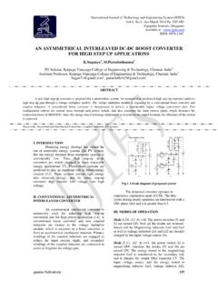
3 Efficiency and Power Loss8331 TA01a FVOUT = 48 VINSW1-2EN/UVLOLT8331 VIN36V TO 72V220 H1M220 H150mA AT VIN = 36V165mA AT VIN = 48V190mA AT VIN = 72 F 41 F 2 VRTINTVCCEFFICIENCYPOWER LOSSVIN = 36 VVIN = 48 VVIN = 72 VLOAD CURRENT (mA) (%)POWER LOSS (W)8331 TA01bLT833128331faFor more information ..140 VVIN, EN/UVLO ..100 VBIAS ..60 VEN/UVLO Pin Above VIN Pin, (Note 2) ..4 VFBX .. 4 VOperating Junction Temperature (Note 3) LT8331E, LT8 331I .. 40 C to 125 CStorage Temperature Range .. 65 C to 150 CLead Temperature (Soldering, 10 sec) ..300 CORDER INFORMATIONLEAD FREE FINISHTAPE AND REELPART MARKING*PACKAGE DESCRIPTIONTEMPERATURE RANGELT8331 EMSE#PBFLT8331 EMSE#TRPBF833116-Lead Plastic MSOP with 4 Pins Removed 40 C to 125 CLT8331 IMSE#PBFLT8331 IMSE#TRPBF833116-Lead Plastic MSOP with 4 Pins Removed 40 C to 125 CConsult LTC Marketing for parts specified with wider operating temperature ranges.
4 *The temperature grade is identified by a label on the shipping container. For more information on lead free part marking, go to: For more information on tape and reel specifications, go to: Some packages are available in 500 unit reels through designated sales channels with #TRMPBF 3 5678EN/UVLOVININTVCCNCBIASNC16 14 1211109SW1SW2 SYNC/MODESSRTFBXTOP VIEW17 PGND, GNDMSE PACKAGEVARIATION: MSE16 (12)16-LEAD PLASTIC MSOP JA = 45 C/W, JC = 10 C/W EXPOSED PAD (PIN 17) IS PGND AND GND, MUST BE SOLDERED TO PCBPIN CONFIGURATIONABSOLUTE MAXIMUM RATINGS(Note 1)PARAMETERCONDITIONSMINTYPMAXUNITSVIN Operating Voltage Quiescent Current at ShutdownVEN/UVLO = l1 22 5 A AVEN/UVLO = A AVIN Quiescent CurrentRT = 100kSleep Mode (Not Switching)SYNC = 0V 25 A AActive Mode (Not Switching)SYNC = 0V, BIAS = 0V l780 8401420 1720 A ASYNC = 0V, BIAS = 5V l17 2440 55 A ASYNC = INTVCC, BIAS = 0V l700 8001080 1170 A ASYNC = INTVCC, BIAS = 5V l17 2440 55 A AELECTRICAL CHARACTERISTICS The l denotes the specifications which apply over the full operating temperature range, otherwise specifications are at TA = 25 C.
5 VIN = 12V, EN/UVLO = 12V unless otherwise #orderinfoLT833138331faFor more information CHARACTERISTICS The l denotes the specifications which apply over the full operating temperature range, otherwise specifications are at TA = 25 C. VIN = 12V, EN/UVLO = 12V unless otherwise 1: Stresses beyond those listed under Absolute Maximum Ratings may cause permanent damage to the device. Exposure to any Absolute Maximum Rating condition for extended periods may affect device reliability and 2: INTVCC cannot be externally driven. No external loading is allowed on this 3: The LT8331E is guaranteed to meet performance specifications from 0 C to 125 C junction temperature. Specifications over the 40 C to 125 C operating junction temperature range are assured by design, characterization and correlation with statistical process controls.
6 The LT8331I is guaranteed over the full 40 C to 125 C operating junction temperature range. High junction temperatures degrade operating lifetimes. Operating lifetime is derated at junction temperatures greater than 125 4: The IC includes overtemperature protection that is intended to protect the device during overload conditions. Junction temperature will exceed 150 C when overtemperature protection is active. Continuous operation above the specified maximum operating junction temperature will reduce ThresholdRising, BIAS Can Supply INTVCC Falling, BIAS Cannot Supply INTVCCl VVIN Falling Threshold to Supply INTVCCBIAS = 12 VBIAS Falling Threshold to Supply INTVCCVIN = 12 VVIN RegulationFBX Regulation VoltageFBX > 0V FBX < 0Vl VFBX Line RegulationFBX > 0V, < VIN < 100V FBX < 0V, < VIN < %/VFBX Pin CurrentFBX = , 1010nAOscillatorSwitching Frequency (fOSC)RT = 301k RT = 100k RT = l l92 279 465100 300 500107 321 535kHz kHz kHzMinimum On-TimeSYNC = 0V SYNC = INTVCC165 160290 290ns nsMinimum Off-Time146230nsSYNC/Mode, Mode ThresholdsRising to Select Pulse Skipping Mode Falling to Select Burst Mode Operationl l VSYNC/Mode, Clock ThresholdsRising Falling VfSYNC/fOSC Allowed RatioRT = Pin CurrentSYNC = 2V 4040nASwitchMaximum Switch Current Limit Overcurrent ThresholdDischarges SS RDS(ON)ISW = Switch Leakage CurrentVSW = AEN/UVLO LogicEN/UVLO Pin Threshold (Rising)Start Pin Threshold (Falling)
7 Stop Pin CurrentVEN/UVLO = 4040nASoft-StartSoft-Start Charge CurrentSS = 1V2 ASoft-Start Pull-Down ResistanceFault Condition, SS = LT833148331faFor more information PERFORMANCE CHARACTERISTICSS witching Frequency vs TemperatureSwitching Frequency vs VINN ormalized Switching Frequency vs FBX VoltageSwitch Current Limit vs Duty CycleSwitch Minimum On-Time vs TemperatureSwitch Minimum Off-Time vs TemperatureFBX Positive Regulation Voltagevs TemperatureFBX Negative Regulation Voltage vs TemperatureEN/UVLO Pin Thresholds vs TemperatureVIN = 12 VJUNCTION TEMPERATURE ( C) 50 VOLTAGE (V)8331 G01 VIN = 12 VJUNCTION TEMPERATURE ( C) 50 250255075100125150175 VOLTAGE (V)8331 G02 VIN = 12 VEN/UVLO RISING (TURN-ON)EN/UVLO FALLING (TURN-OFF)JUNCTION TEMPERATURE ( C) 50 PIN VOLTAGE (V)8331 G03 VIN = 12 VJUNCTION TEMPERATURE ( C) 50 2502550751001251501754754804854904955005 05510515520525 SWITCHING FREQUENCY (kHz)8331 G04 VIN (V)0102030405060708090100475480485490495 500505510515520525 SWITCHING FREQUENCY (kHz)8331 G05 VIN = 12 VFBX VOLTAGE (V) SWITCHING FREQUENCY (%)8331 G06 VIN = 12 VDUTY CYCLE (%) CURRENT LIMIT (A)8331 G07 SYNC = 0 VSYNC = INTVCCJUNCTION TEMPERATURE ( C) 50 2502550751001251501751301401501601701801 90200 MINIMUM ON TIME (ns)8331 G08 JUNCTION TEMPERATURE ( C) 50 2502550751001251501751101201301401501601 70180 MINIMUM OFF TIME (ns)8331 G09LT833158331faFor more information PERFORMANCE CHARACTERISTICSS witching Waveforms(in CCM)Switching Waveforms(in DCM/Light Burst Mode)Switching Waveforms(in Deep Burst Mode)Burst Frequency vs Load CurrentVIN Pin Current (Sleep Mode, Not Switching) vs TemperatureVIN Pin Current (Active Mode, Not Switching) vs TemperatureVIN Pin Current (Active Mode, Not Switching)
8 Vs TemperatureVIN = 12 VVSYNC/MODE = 0 VVBIAS = 0 VJUNCTION TEMPERATURE ( C) 50 PIN CURRENT ( A)8331 G10 JUNCTION TEMPERATURE ( C) 50 2502550751001251501756006507007508008509 009501000 VIN PIN CURRENT ( A)8331 G11 VIN = 12 VVSYNC/MODE = 0 VVBIAS = 0 VJUNCTION TEMPERATURE ( C) 50 250255075100125150175051015202530 VIN PIN CURRENT ( A)8331 G12 VIN = 12 VVSYNC/MODE = 0 VVBIAS = 5 VVOUT Transient Response: LoadCurrent Transients from to 165mA to Transient Response: LoadCurrent Transients from 5mA to 165mA to 5mA2 s/DIVVSW50V/DIVIL1+IL2200mA/DIV8331 G13 FRONT PAGE APPLICATIONVIN = 48V, VOUT = 48V, ILOAD = 165mA2 s/DIVVSW50V/DIVIL1+IL2200mA/DIV8331 G14 FRONT PAGE APPLICATIONVIN = 48V, VOUT = 48V, ILOAD = 15mA5 s/DIVVSW50V/DIVIL1+IL2200mA/DIV8331 G15 FRONT PAGE APPLICATIONVIN = 48V, VOUT = 48V, ILOAD = 3mAFRONT PAGE APPLICATIONVIN = 48V, VOUT = 48 VLOAD CURRENT (mA)0204060801000150300450600 SWITCHING FREQUENCY (kHz)8331 G16 FRONT PAGE APPLICATIONVIN = 48V, VOUT = 48V200 s/DIVVOUT500mV/DIVILOAD100mA/DIV8331 G17 FRONT PAGE APPLICATIONVIN = 48V, VOUT = 48V500 s/DIVVOUT1V/DIVILOAD100mA/DIV8331 G18LT833168331faFor more information FUNCTIONSEN/UVLO (Pin 1): Shutdown and Undervoltage Detect Pin.
9 The LT8331 is shut down when this pin is low and active when this pin is high. Below an accurate threshold, the part enters undervoltage lockout and stops switching. This allows an undervoltage lockout (UVLO) threshold to be programmed for system input voltage by resistively dividing down system input voltage to the EN/UVLO pin. A 140mV pin hysteresis ensures part switching resumes when the pin exceeds EN/UVLO pin voltage below reduces VIN current below 1 A. If shutdown and UVLO features are not required, the pin can be tied directly to system (Pin 3): Input Supply. This pin must be locally bypassed. Be sure to place the positive terminal of the input capaci-tor as close as possible to the VIN pin, and the negative terminal as close as possible to the exposed pad PGND copper (near Pin 1).INTVCC (Pin 5): Regulated Supply for Internal Loads. The INTVCC pin must be bypassed with a minimum 1 F low ESR ceramic capacitor to GND.
10 No additional components or loading is allowed on this pin. INTVCC draws power from the BIAS pin if BIAS VIN , otherwise INTVCC is powered by the VIN (Pins 6, 8): No Internal Connection. Leave these pins (Pin 7): Second Input Supply for Powering INTVCC. Removes the majority of INTVCC current from the VIN pin to improve efficiency when BIAS VIN If unused, tie the pin to GND (Pin 9): Voltage Regulation Feedback Pin for Positive or Negative Outputs. Connect this pin to a resistor divider between the output and the exposed pad GND copper (near Pin 9). FBX reduces the switching frequency during start-up and fault conditions when FBX is close to (Pin 10): A resistor from this pin to the exposed pad GND copper (near Pin 9) programs switching (Pin 11): Soft-Start Pin. Connect a capacitor from this pin to GND copper (near Pin 9) to control the ramp rate of inductor current during converter start-up.