Transcription of Application Note 24 A Simplified Test Set for Op Amp ...
1 LM709. Application Note 24 A Simplified Test Set for Op Amp characterization Literature Number: SNOA637. A Simplified Test Set for Op Amp characterization AN-24. National Semiconductor A Simplified Test Set for Application Note 24. M. Yamatake Op Amp characterization April 1986. INTRODUCTION POWER SUPPLY. The test set described in this paper allows complete quanti- Basic waveforms and dc operating voltages for the test set tative characterization of all dc operational amplifier param- are derived from a power supply section comprising a posi- eters quickly and with a minimum of additional equipment. tive and a negative rectifier and filter, a test set voltage regu- The method used is accurate and is equally suitable for labo- lator, a test circuit voltage regulator, and a function genera- ratory or production test for quantitative readout or for limit tor.
2 The dc supplies will be discussed in the section dealing testing. As embodied here, the test set is conditioned for with detailed circuit description. testing the LM709 and LM101 amplifiers; however, simple The waveform generator provides three output functions, a changes discussed in the text will allow testing of any of the 19V square wave, a 19V to +19V pulse with a 1% duty generally available operational amplifiers. cycle, and a 5V triangular wave. The square wave is the Amplifier parameters are tested over the full range of com- basic waveform from which both the pulse and triangular mon mode and power supply voltages with either of two out- wave outputs are derived.
3 Put loads. Test set sensitivity and stability are adequate for The square wave generator is an operational amplifier con- testing all presently available integrated amplifiers. nected as an astable multivibrator. This amplifier provides an The paper will be divided into two sections, , a functional output of approximately 19V at 16 Hz. This square wave is description, and a discussion of circuit operation. Complete used to drive junction FET switches in the test set and to construction information will be given including a layout for generate the pulse and triangular waveforms. the tester circuit boards. The pulse generator is a monostable multivibrator driven by the output of the square wave generator.
4 This multivibrator is FUNCTIONAL DESCRIPTION allowed to swing from negative saturation to positive satura- The test set operates in one of three basic modes. These tion on the positive going edge of the square wave input and are: (1) Bias Current Test; (2) Offset Voltage, Offset Current has a time constant which will provide a duty cycle of ap- Test; and (3) Transfer Function Test. In the first two of these proximately 1%. The output is approximately 19V to +19V. tests, the amplifier under test is exercised throughout its full common mode range. In all three tests, power supply volt- ages for the circuit under test may be set at 5V, 10V, 15V, or 20V. AN007190-1.
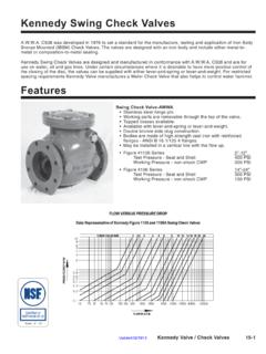
5 FIGURE 1. Functional Diagram of Bias Current Test Circuit The triangular wave generator is a dc stabilized integrator The purpose of these various outputs from the power supply driven by the output of the square wave generator and pro- section will be discussed in the functional description. AN-24. vides a 5V output at the square wave frequency, inverted with respect to the square wave. 1998 National Semiconductor Corporation AN007190 1. PrintDate=1998/04/24 PrintTime=08:34:00 39684 an007190 Rev. No. 3 cmserv Proof 1. BIAS CURRENT TEST The bias current display of Figure 2 has the added advan- A functional diagram of the bias current test circuit is shown tage that incipient breakdown of the input stage of the device in Figure 1.
6 The output of the triangular wave generator and under test at the extremes of the common mode range is the output of the test circuit, respectively, drive the horizontal easily detected. and vertical deflection of an oscilloscope. If either or both the upper or lower trace in the bias current The device under test, (cascaded with the integrator, A7), is display exhibits curvature near the horizontal ends of the os- connected in a differential amplifier configuration by R1, R2, cilloscope face, then the bias current of that input of the am- R3, and R4. The inputs of this differential amplifier are driven plifier is shown to be dependent on common mode voltage.
7 In common from the output of the triangular wave generator The usual causes of this dependency are low breakdown through attenuator R8 and amplifier A8. The inputs of the de- voltage of the differential input stage or current sink. vice under test are connected to the feedback network through resistors R5 and R6, shunted by the switch S5a and OFFSET VOLTAGE, OFFSET CURRENT TEST. S5b. The offset voltage and offset current tests are performed in The feedback network provides a closed loop gain of 1,000 the same general way as the bias current test. The only dif- and the integrator time constant serves to reduce noise at ference is that the switches S5a and S5b are closed on the the output of the test circuit as well as allowing the output of same half-cycle of the triangular wave input.
8 The device under test to remain near zero volts. The synchronous operation of S5a and S5b forces the ampli- The bias current test is accomplished by allowing the device fier under test to draw its input currents through matched under test to draw input current to one of its inputs through high and low input resistors on alternate halves of the input the corresponding input resistor on positive going or nega- triangular wave. The difference between the voltage drop tive going halves of the triangular wave generator output. across the two values of input resistors is proportional to the This is accomplished by closing S5a or S5b on alternate difference in input current to the two inputs of the amplifier halves of the triangular wave input.
9 The voltage appearing under test and may be measured as the vertical spacing be- across the input resistor is equal to input current times the in- tween the two traces appearing on the face of the oscillo- put resistor. This voltage is multiplied by 1,000 by the feed- scope. back loop and appears at the integrator output and the ver- Offset voltage is measured as the vertical spacing between tical input of the oscilloscope. The vertical separaton of the the trace corresponding to one of the two values of source traces representing the two input currents of the amplifier un- resistance and the zero volt baseline. Switch S6 and Resis- der test is equivalent to the total bias current of the amplifier tor R9 are a base line chopper whose purpose is to provide under test.
10 A baseline reference which is independent of test set and os- The bias current over the entire common mode range may cilloscope drift. S6 is driven from the pulse output of the func- be examined by setting the output of A8 equal to the amplifier tion generator and has a duty cycle of approximately 1% of common mode range. A photograph of the bias current oscil- the triangular wave. loscope display is given as Figure 2. In this figure, the total Figure 3 is a photograph of the various waveforms presented input current of an amplifier is displayed over a 10V com- during this test. Offset voltage and offset current are dis- mon mode range with a sensitivity of 100 nA per vertical played at a sensitivity of 1 mV and 100 nA per division, re- division.