Transcription of BSS138 - onsemi.cn
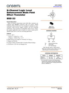
1 DATA SHEET. N- channel Logic Level D. enhancement Mode field effect Transistor G. BSS138 S. General Description These N channel enhancement mode field effect transistors are produced using onsemi's proprietary, high cell density, DMOS. technology. These products have been designed to minimize on state resistance while provide rugged, reliable, and fast switching SOT 23 3. performance. These products are particularly suited for low voltage, CASE 318 08. low current applications such as small servo motor control, power MOSFET gate drivers, and other switching applications. MARKING DIAGRAM. Features A, 50 V 3. RDS(on) = @ VGS = 10 V Drain RDS(on) = @ VGS = V. SSMG. High Density Cell Design for Extremely Low RDS(on) G.
2 Rugged and Reliable Compact Industry Standard SOT 23 Surface Mount Package 1 2. This Device is Pb Free and Halogen Free Gate Source SS = Specific Device Code M = Date Code*. G = Pb Free Package (Note: Microdot may be in either location). *Date Code orientation and/or position may vary depending upon manufacturing location. ORDERING INFORMATION. Device Package Shipping . BSS138 , SOT 23 3 3000 /. BSS138 G (Pb Free) Tape & Reel For information on tape and reel specifications, including part orientation and tape sizes, please refer to our Tape and Reel Packaging Specification Brochure, BRD8011/D. Semiconductor Components Industries, LLC, 2005 1 Publication Order Number: November, 2021 Rev. 6 BSS138 /D. BSS138 .
3 ABSOLUTE MAXIMUM RATINGS TA = 25 C unless otherwise noted. Symbol Parameter Ratings Unit VDSS Drain Source Voltage 50 V. VGSS Gate Source Voltage 20. ID Drain Current Continuous (Note 1) A. Drain Current Pulsed (Note 1) PD Maximum Power Dissipation (Note 1) W. Derate Above 25 C mW/ C. TJ, TSTG Operating and Storage Junction Temperature Range 55 to +150 C. TL Maximum Lead Temperature for Soldering Purposes, 1/16 from Case 300. for 10 s Stresses exceeding those listed in the Maximum Ratings table may damage the device. If any of these limits are exceeded, device functionality should not be assumed, damage may occur and reliability may be affected. THERMAL CHARACTERISTICS TA = 25 C unless otherwise noted. Symbol Parameter Ratings Unit R JA Thermal Resistance, Junction to Ambient (Note 1) 350 C/W.
4 ELECTRICAL CHARACTERISTICS TA = 25 C unless otherwise noted. Symbol Parameter Test Conditions Min Typ Max Unit OFF CHARACTERISTICS. BVDSS Drain Source Breakdown Voltage VGS = 0 V, ID = 250 A 50 V. V GS(th) Breakdown Voltage Temperature ID = 250 A, Referenced to 72 mV/ C. Coefficient 25 C. T J. IDSS Zero Gate Voltage Drain Current VDS = 50 V, VGS = 0 V A. VDS = 50 V, VGS = 0 V, 5. TJ = 125 C. VDS = 30 V, VGS = 0 V 100 nA. IGSS Gate Body Leakage VGS = 20 V, VDS = 0 V 100. ON CHARACTERISTICS. VGS(th) Gate Threshold Voltage VDS = VGS, ID = 1 mA V. V GS(th) Gate Threshold Voltage Temperature ID = 1 mA, Referenced to 25 C 2 mV/ C. Coefficient T J. RDS(on) Static Drain Source On Resistance VGS = 10 V, ID = A . VGS = V, ID = A.
5 VGS = 10 V, ID = A, TJ = 125 C. ID(on) On State Drain Current VGS = 10 V, VDS = 5 V A. gFS Forward Transconductance VDS = 10 V, ID = A S. DYNAMIC CHARACTERISTICS. Ciss Input Capacitance VDS = 25 V, VGS = 0 V, 27 pF. f = MHz Coss Output Capacitance 13 pF. Crss Reverse Transfer Capacitance 6 pF. RG Gate Resistance VGS = 15 mV, f = MHz 9 . 2. BSS138 . ELECTRICAL CHARACTERISTICS TA = 25 C unless otherwise noted. (continued). Symbol Parameter Test Conditions Min Typ Max Unit SWITCHING CHARACTERISTICS. td(on) Turn On Delay Time VDD = 30 V, ID = A, 5 ns VGS = 10 V, RGEN = 6 . tr Turn On Rise Time 9 18 ns td(off) Turn Off Delay Time 20 36 ns tf Turn Off Fall Time 7 14 ns Qg Total Gate Charge VDS = 25 V, ID = A, nC.
6 VGS = 10 V. Qgs Gate Source Charge nC. Qgd Gate Drain Charge nC. DRAIN SOURCE DIODE CHARACTERISTICS AND MAXIMUM RATINGS. IS Maximum Continuous Drain Source Diode Forward Current A. VSD Drain Source Diode Forward Voltage VGS = 0 V, IS = A (Note 2) V. Product parametric performance is indicated in the Electrical Characteristics for the listed test conditions, unless otherwise noted. Product performance may not be indicated by the Electrical Characteristics if operated under different conditions. 1. R JA is the sum of the junction to case and case to ambient thermal resistance where the case thermal reference is defined as the solder mounting surface of the drain pins. R JA is guaranteed by design while R JA is determined by the user's board design.
7 A) 350 C/W when mounted on a minimum pad. 2. Pulse Test: Pulse Width 300 s, Duty Cycle TYPICAL CHARACTERISTICS. 1 VGS = 10 V V V. 3. Drain Source On Resistance V VGS = V. 9V. ID, Drain Current (A). RDS(on), Normalized V. V. V V. V. V. 10 V. V 1. 0 0 1 2 3 0 1. VDS, Drain To Source Voltage (V) ID, Drain Current (A). Figure 1. On Region Characteristics Figure 2. On Resistance Variation with Drain Current and Gate Voltage 3. BSS138 . TYPICAL CHARACTERISTICS (continued). 2 ID = 220 mA ID = 110 mA. Drain Source On Resistance RDS(on), On Resistance (W). VGS = 10 V. RDS(on), Normalized TA = 125 C. 1. TA = 25 C. 50 25 0 25 50 75 100 125 150 0 2 4 6 8 10. TJ, Junction Temperature (5C) VGS, Gate To Source Voltage (V).
8 Figure 3. On Resistance Variation with Temperature Figure 4. On Resistance Variation with Gate to Source Voltage 1. 25 C VGS = 0 V. VDS = 10 V TA = 55 C. IS, Reverse Drain Current (A). TA = 125 C. 125 C ID, Drain Current (A). 25 C 55 C. 0 1 2 3 0 1 VGS, Gate To Source Voltage (V) VSD, Body Diode Forward Voltage (V). Figure 5. Transfer Characteristics Figure 6. Body Diode Forward Voltage Variation with Source Current and Temperature 10 100. ID = 220 mA. VDS = 8 V. VGS, Gate Source Voltage (V). 25 V. 8 80. Capacitance (pF). 30 V. 6 60. 4 40. CISS. COSS. 2 20. CRSS. 0 0. 0 1 0 10 20 30 40 50. Qg, Gate Charge (nC) VSD, Drain To Source Voltage (V). Figure 7. Gate Charge Characteristics Figure 8. Capacitance Characteristics 4.
9 BSS138 . 10 5. Single Pulse P(pk), Peak Transient Power (W). R JA = 350 C/W. 100 s 4 TA = 25 C. 1. ID, Drain Current (A). RDS(on) Limit 1 ms 10 ms 3. 100 ms 2. VGS = 10 V 1s Single Pulse DC 1. R JA = 350 C/W. TA = 25 C. 0. 0 1 10 100 1 10 100 1000. VDS, Drain Source Voltage (V) t1, Time (s). Figure 9. Maximum Safe Operating Area Figure 10. Single Pulse Maximum Power Dissipation 1. r(t), Normalized Effective Transient D = Thermal Resistance R JA(t)= r(t) * R JA. R JA = 350 C/W. P(pk). t1. Single Pulse t2. TJ TA = P * R JA(t). Duty Cycle, D = t1 / t2. 1 10 100 1000. t1, Time (s). Figure 11. Transient Thermal Response Curve Thermal characterization performed using the conditions described in Note 1a. Transient thermal response will change depending on the circuit board design.
10 5. MECHANICAL CASE OUTLINE. PACKAGE DIMENSIONS. SOT 23 (TO 236). CASE 318 08. ISSUE AS. DATE 30 JAN 2018. SCALE 4:1. D NOTES: 1. DIMENSIONING AND TOLERANCING PER ASME , 1994. 2. CONTROLLING DIMENSION: MILLIMETERS. 3. MAXIMUM LEAD THICKNESS INCLUDES LEAD FINISH. MINIMUM LEAD THICKNESS IS THE MINIMUM THICKNESS OF. 3 THE BASE MATERIAL. 4. DIMENSIONS D AND E DO NOT INCLUDE MOLD FLASH, E HE T PROTRUSIONS, OR GATE BURRS. 1 2. MILLIMETERS INCHES. DIM MIN NOM MAX MIN NOM MAX. L A 3X b A1 L1 b e VIEW C c TOP VIEW D E e L L1 A HE T 0 10 0 10 . A1 SIDE VIEW SEE VIEW C c GENERIC. END VIEW. MARKING DIAGRAM*. RECOMMENDED. SOLDERING FOOTPRINT XXXMG. G. 1. 3X. XXX = Specific Device Code M = Date Code G = Pb Free Package *This information is generic.