Transcription of Digital FET, N-Channel - ON Semiconductor
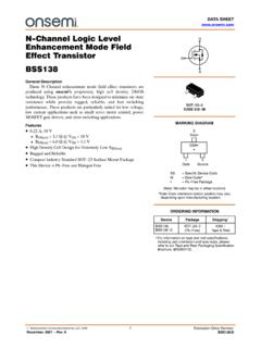
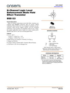
1 Semiconductor Components Industries, LLC, 1997 March, 2020 Rev. 51 Publication Order Number:FDV303N/DDigital FET, N-ChannelFDV303 NGeneral DescriptionThese N channel enhancement mode field effect transistors areproduced using ON Semiconductor s proprietary, high cell density,DMOS technology. This very high density process is tailored tominimize on state resistance at low gate drive conditions. This deviceis designed especially for application in battery circuits using eitherone lithium or three cadmium or NMH cells. It can be used as aninverter or for high efficiency miniature discrete DC/DC conversionin compact portable electronic devices like cellular phones and device has excellent on state resistance even at gate drivevoltages as low as 25 V, A Continuous, 2 A Peak RDS(ON) = @ VGS = V RDS(ON) = @ VGS= V Very Low Level Gate Drive Requirements Allowing Direct Operationin 3 V Circuits, VGS(th)
2 < 1 V Gate Source Zener for ESD Ruggedness, > 6 kV Human BodyModel Compact Industry Standard SOT 23 Surface Mount Package This Device is Pb Free, Halogen Free/BFR Free and is RoHSCompliant* Location code can be blank or with charactersindicating manufacturing location* Date Code orientation and overbar may vary depending upon manufacturing detailed ordering and shipping information on page 2 ofthis data INFORMATIONMARKING DIAGRAMSOT 23 (TO 236)CASE 318 08 STYLE 21 PIN ASSIGNMENTAor blank = One/two character Loacation Code303= Specific Device CodeM= Date CodeG= Pb Free PackageSOT 231A303 MGGDGS(Note: Microdot may be in either location) MAXIMUM RATINGS TA = 25 C unless otherwise notedSymbolParameterFDV303 NUnitsVDSSD rain Source Voltage, Power Supply Voltage25 VVGSSGate Source Voltage, VIN8 VIDD rain/Output Current Continuous Power , TSTGO perating and Storage Temperature Range 55 to 150 CESDE lectrostatic Discharge Rating MIL STD 883D Human Body Model (100 pf / 1500 W)
3 CHARACTERISTICSS ymbolParameterRatingsUnitsR JAThermal Resistance, Junction to Ambient357 C/WORDERING INFORMATION DevicePackageShipping FDV303 NSOT 23 Case 318 083000 / Tape & Reel For information on tape and reel specifications, including part orientation and tape sizes, please refer to our Tape and Reel PackagingSpecifications Brochure, BRD8011 CHARACTERISTICS TJ = 25 C unless otherwise notedSymbolParameterConditionsMinTypMaxU nitsOFF CHARACTERISTICSBVDSSD rain Source Breakdown VoltageVGS = 0 V, ID = 250 mA25V BVDSS/ TJBreakdown Voltage Temp. CoefficientID = 250 mA, Referenced to 25 C26mV/ CIDSSZero Gate Voltage Drain CurrentVDS = 20 V, VGS = 0 V1mATJ = 55 C10mAIGSSGate Body Leakage CurrentVGS = 8 V, VDS= 0 V100nAON CHARACTERISTICS (Note 1) VGS(th)/ TJGate Threshold Voltage TemperatureCoefficientID = 250 mA, Referenced to 25 C CVGS(th)Gate Threshold VoltageVDS = VGS, ID = 250 (ON)Static Drain Source On ResistanceVGS = V, ID = TJ =125 = V, ID = (ON)On State Drain CurrentVGS = V, VDS = 5 TransconductanceVDS = 5 V, ID= CHARACTERISTICSCissInput CapacitanceVDS = 10 V, VGS = 0 V, f = MHz50pFCossOutput Capacitance28pFCrssReverse Transfer Capacitance9pFSWITCHING CHARACTERISTICS (Note 1)tD(on)Turn On Delay TimeVDD = 6 V, ID = A, VGS = V, RGEN = 50 36nstrTurn On Rise (off)
4 Turn Off Delay Time1730nstfTurn Off Fall Time1325nsQgTotal Gate ChargeVDS = 5 V, ID = A, VGS = Source Drain SOURCE DIODE CHARACTERISTICS AND MAXIMUM RATINGSISM aximum Continuous Drain Source Diode Forward Source Diode Forward VoltageVGS = 0 V, IS = A (Note 1) Pulse Test: Pulse Width < 300 ms, Duty Cycle < CHARACTERISTICSF igure 1. On Region CharacteristicsFigure 2. On Resistance Variation withDrain Current and Gate VoltageFigure 3. On Resistance Variationwith TemperatureFigure 4. On Resistance Variation withGate To Source VoltageFigure 5. Transfer CharacteristicsFigure 6. Body Diode Forward VoltageVariation with Source Current and , DRAIN SOURCE VOLTAGE (V) I , DRAIN SOURCE CURRENT (A) = (on), , DRAIN CURRENT (A)DRAIN SOURCE ON RESISTANCEV = 50 25025 50 75100 125 , JUNCTION TEMPERATURE ( C)DRAIN SOURCE ON RESISTANCEV = VGSI = ADR , NORMALIZEDDS(ON) , GATE TO SOURCE VOLTAGE (V)I , DRAIN CURRENT (A)25 C125 CV = VDSGSTJ = 55 , BODY DIODE FORWARD VOLTAGE (V)I , REVERSE DRAIN CURRENT (A)TJ = 125 C25 C 55 CV = 0 , GATE TO SOURCE VOLTAGE (V) ID= , ON RESISTANCE DS(on) 125 C 25 C(W)
5 = CHARACTERISTICS TJ = 25 C Unless Otherwise Noted (continued)Figure 7. Gate Charge CharacteristicsFigure 8. Capacitance CharacteristicsFigure 9. Maximum Safe Operating AreaFigure 10. Single Pulse Maximum PowerDissipationFigure 11. Transient Thermal Response , GATE CHARGE (nC)V , GATE SOURCE VOLTAGE (V)gGSI = AD10 V15 VV = 5 V , DRAI N SOURCE VOLTAGE (V)I , DRAIN CURRENT (A)V = VSINGLE PULSER = 357 C/WT = 25 CGS PULSE TIME (s)POWER (W)SINGLE PULSER = 357 C/WT = 25 C , TIME (sec)TRANSIENT THERMAL RESISTANCEDuty Cycle, D = t /t12R (t)= r(t) * R R = 357 C/W JA JA JAT T = P * R (t) JAAJP(pk) t1 t2r(t), NORMALIZED EFFECTIVE1 Single Pulse D = 510255102050100150V , DRAIN TO SOURCE VOLTAGE (V)CAPACITANCE (pF)DSCissf = 1 MHzV = 0 VGSCossCrssSOT 23 (TO 236)CASE 318 08 ISSUE ASDATE 30 JAN 2018 SCALE 4.
6 1DA13121 XXXMGGXXX = Specific Device CodeM= Date CodeG= Pb Free Package*This information is generic. Please refer todevice data sheet for actual part Free indicator, G or microdot G ,may or may not be DIAGRAM*NOTES:1. DIMENSIONING AND TOLERANCING PER ASME , CONTROLLING DIMENSION: MAXIMUM LEAD THICKNESS INCLUDES LEAD LEAD THICKNESS IS THE MINIMUM THICKNESS OFTHE BASE DIMENSIONS D AND E DO NOT INCLUDE MOLD FLASH,PROTRUSIONS, OR GATE FOOTPRINTVIEW VIEW 22:PIN 1. RETURN2. OUTPUT3. INPUTSTYLE 6:PIN 1. BASE2. EMITTER3. COLLECTORSTYLE 7:PIN 1. EMITTER2. BASE3. COLLECTORSTYLE 8:PIN 1. ANODE2. NO CONNECTION3. CATHODESTYLE 9:PIN 1. ANODE2. ANODE3. CATHODESTYLE 10:PIN 1. DRAIN2. SOURCE3. GATESTYLE 11:PIN 1. ANODE2.
7 CATHODE3. CATHODE ANODESTYLE 12:PIN 1. CATHODE2. CATHODE3. ANODESTYLE 13:PIN 1. SOURCE2. DRAIN3. GATESTYLE 14:PIN 1. CATHODE2. GATE3. ANODESTYLE 15:PIN 1. GATE2. CATHODE3. ANODESTYLE 16:PIN 1. ANODE2. CATHODE3. CATHODESTYLE 17:PIN 1. NO CONNECTION2. ANODE3. CATHODESTYLE 18:PIN 1. NO CONNECTION2. CATHODE3. ANODESTYLE 19:PIN 1. CATHODE2. ANODE3. CATHODE ANODESTYLE 23:PIN 1. ANODE2. ANODE3. CATHODESTYLE 20:PIN 1. CATHODE2. ANODE3. GATESTYLE 21:PIN 1. GATE2. SOURCE3. DRAINSTYLE 1 THRU 5:CANCELLEDSTYLE 24:PIN 1. GATE 2. DRAIN 3. SOURCESTYLE 25:PIN 1. ANODE 2. CATHODE 3. GATESTYLE 26:PIN 1. CATHODE 2. ANODE 3. NO CONNECTIONSTYLE 27:PIN 1. CATHODE 2. CATHODE 3. 100 10T T3 XTOP VIEWSIDE VIEWEND : 28:PIN 1.
8 ANODE 2. ANODE 3. ANODEMECHANICAL CASE OUTLINEPACKAGE DIMENSIONSON Semiconductor and are trademarks of Semiconductor Components Industries, LLC dba ON Semiconductor or its subsidiaries in the United States and/or other Semiconductor reserves the right to make changes without further notice to any products herein. ON Semiconductor makes no warranty, representation or guarantee regardingthe suitability of its products for any particular purpose, nor does ON Semiconductor assume any liability arising out of the application or use of any product or circuit, and specificallydisclaims any and all liability, including without limitation special, consequential or incidental damages. ON Semiconductor does not convey any license under its patent rights nor therights of NUMBER:DESCRIPTION:Electronic versions are uncontrolled except when accessed directly from the Document versions are uncontrolled except when stamped CONTROLLED COPY in 1 OF 1 SOT 23 (TO 236) Semiconductor Components Industries, LLC, , , and other names, marks, and brands are registered and/or common law trademarks of Semiconductor Components Industries, LLC dba onsemi or its affiliatesand/or subsidiaries in the United States and/or other countries.
9 Onsemi owns the rights to a number of patents, trademarks, copyrights, trade secrets, and other intellectual listing of onsemi s product/patent coverage may be accessed at onsemi reserves the right to make changes at any time to anyproducts or information herein, without notice. The information herein is provided as is and onsemi makes no warranty, representation or guarantee regarding the accuracy of theinformation, product features, availability, functionality, or suitability of its products for any particular purpose, nor does onsemi assume any liability arising out of the application or useof any product or circuit, and specifically disclaims any and all liability, including without limitation special, consequential or incidental damages. Buyer is responsible for its productsand applications using onsemi products, including compliance with all laws, regulations and safety requirements or standards, regardless of any support or applications informationprovided by onsemi.
10 Typical parameters which may be provided in onsemi data sheets and/or specifications can and do vary in different applications and actual performance mayvary over time. All operating parameters, including Typicals must be validated for each customer application by customer s technical experts. onsemi does not convey any licenseunder any of its intellectual property rights nor the rights of others. onsemi products are not designed, intended, or authorized for use as a critical component in life support systemsor any FDA Class 3 medical devices or medical devices with a same or similar classification in a foreign jurisdiction or any devices intended for implantation in the human body. ShouldBuyer purchase or use onsemi products for any such unintended or unauthorized application, Buyer shall indemnify and hold onsemi and its officers, employees, subsidiaries, affiliates,and distributors harmless against all claims, costs, damages, and expenses, and reasonable attorney fees arising out of, directly or indirectly, any claim of personal injury or deathassociated with such unintended or unauthorized use, even if such claim alleges that onsemi was negligent regarding the design or manufacture of the part.