Transcription of Field Effect Transistors - Learn About Electronics
1 SEMICONDUCTORS 1 E. COATES 2016 Field Effect Transistors Module Junction Field Effect Transistors Field Effect Transistors Although there are lots of confusing names for Field Effect Transistors (FETs) there are basically two main types: 1. The reverse biased PN junction types, the JFET or Junction FET, (also called the JUGFET or Junction Unipolar Gate FET). 2. The insulated gate FET devices (IGFET).
2 All FETs can be called UNIPOLAR devices because the charge carriers that carry the current through the device are all of the same type either holes or electrons, but not both. This distinguishes FETs from the bipolar devices in which both holes and electrons are responsible for current flow in any one device. The JFET This was the earliest FET device available. It is a voltage-controlled device in which current flows from the SOURCE terminal (equivalent to the emitter in a bipolar transistor ) to the DRAIN (equivalent to the collector).
3 A voltage applied between the source terminal and a GATE terminal (equivalent to the base) is used to control the source - drain current. The main difference between a JFET and a bipolar transistor is that in a JFET no gate current flows, the current through the device is controlled by an electric Field , hence " Field Effect transistor ". The JFET construction and circuit symbols are shown in Figures 1, 2 and 3. Module 4 What you ll Learn in Module 4 Section Field Effect Transistors .
4 FETs JFETs, JUGFETs, and IGFETS The JFET. Diffusion JFET Construction. Planar JFET Construction. JFET Circuit Symbols. Section How a JFET Works. Operation Below Pinch Off. Operation Above Pinch Off. JFET Output Characteristic. JFET Transfer Characteristic. JFET Video. Section The enhancement Mode MOSFET. The IGFET (Insulated Gate FET). MOSFET(IGFET) Construction. MOSFET(IGFET) Operation. MOSFET (IGFET) Circuit Symbols. Handling Precautions for MOSFETS Section The Depletion Mode MOSFET.
5 Depletion Mode MOSFET Operation. MOSFE (IGFET) Circuit Symbols. Applications of MOSFETS High Power MOSFETS Section Power MOSFETs. MOSFET Calculations. Choosing a MOSFET Section MOSFET Switches. Design and Build typical MOSFET Switch Circuits. Section FET Quiz. Check your understanding of Field Effect Transistors . Semiconductors Module 4 Field Effect Transistors SEMICONDUCTORS MODULE 4 PDF 2 E.
6 COATES 2020 JFET Construction The construction of JFETs can be theoretically quite simple, but in reality difficult, requiring very pure materials and clean room techniques. JFETs are made in different forms, some being made as discrete (single) components and others, using planar technology as integrated circuits. Fig. shows the (theoretically) simplest form of construction for a Junction FET (JFET) using diffusion techniques. It uses a small slab of N type semiconductor into which are infused two P type areas to form the Gate.
7 Current in the form of electrons flows through the device from source to drain along the N type silicon channel . As only one type of charge carrier (electrons) carry current in N channel JFETs, these Transistors are also called "Unipolar" devices. Fig. shows the cross section of a N channel planar Junction FET (JFET) The load current flows through the device from source to drain along a channel made of N type silicon. In the planar device the second part of the gate is formed by the P type substrate.
8 JFET Circuit Symbols P channel JFETs are also available and the principle of operation is the same as the N channel type described here, but polarities of the voltages are of course reversed, and the charge carriers are holes. Notice in the JFET circuit symbols shown in Fig. that the arrowhead on the gate connection always points towards the negative connection, indicating the polarity (either P or N channel ) of the channel . Semiconductors Module 4 Field Effect Transistors SEMICONDUCTORS MODULE 4 PDF 3 E.
9 COATES 2020 Module How a JFET Works The JFET is a Voltage Controlled transistor . The JFET is a voltage controlled transistor that has two distinct areas of operation depending on the whether the voltage applied to the Source and Drain terminals is greater or less that the transistor 's Pinch-Off Voltage The Pinch Off Voltage The Pinch-Off value of the JFET refers to the voltage applied between Drain and Source (with the Gate voltage at zero volts) at which maximum current flows.
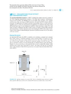
10 Operating with the Drain/Source voltage below this value is classed is the "Ohmic Region" as the JFET will act rather like a resistor. Operating with the Drain Source voltage above Pinch Off is known as the "Saturation Region" as the JFET is acting like a saturated transistor ; that is any increase in voltage does not produce a relative increase in current. Operation Below Pinch Off In the planar construction N channel JFET shown in Fig. , the N channel is sandwiched between two P type regions (the gate and the substrate) that are connected together and are at 0V.