Example: barber
CD4066B CMOS Quad Bilateral Switch datasheet (Rev. H)
CD4066B CMOS Quad Bilateral Switch 1 1 Features 1• 15-V Digital or ±7.5-V Peak-to-Peak Switching • 125-ΩTypical On-State Resistance for 15-V Operation • Switch On-State Resistance Matched to Within 5 ΩOver 15-V Signal-Input Range • On-State Resistance Flat Over Full Peak-to-Peak Signal Range • High On or Off Output-Voltage Ratio:
Tags:
Information
Domain:
Source:
Link to this page:
Documents from same domain

1.8-V Micropower CMOS Operational Amplifier …
www.ti.com5 OPA2333-HT www.ti.com SBOS483I –JULY 2009–REVISED MAY 2015 Product Folder Links: OPA2333-HT Copyright © 2009–2015, Texas Instruments Incorporated Submit Documentation Feedback

LMC6482 CMOS Dual Rail-To-Rail Input and Output ...
www.ti.comLMC6482 www.ti.com SNOS674E –NOVEMBER 1997–REVISED APRIL 2015 5 Pin Configuration and Functions D, DGK and P Packages 8-Pin SOIC, VSSOP and PDIP (Top View) Pin Functions PIN TYPE DESCRIPTION NO.

OPAx354 250-MHz, Rail-to-Rail I/O, CMOS …
www.ti.comOPA354 IN +IN V OUT V+ V Product Folder Order Now Technical Documents Tools & Software Support & Community Reference Design An IMPORTANT NOTICE at the end of this data sheet addresses availability, warranty, changes, use …

LM136-2.5,LM236-2.5,LM336-2 - TI.com
www.ti.comLM136-2.5/LM236-2.5/LM336-2.5V Reference Diode General Description The LM136-2.5/LM236-2.5 and LM336-2.5 integrated cir-cuits are …

SimpleLink™ CC3120, CC3220 Wi-Fi ... - Texas …
www.ti.comUser User x x x x x x x x x x x x x x x x x x x x Application Servers Vendor IoT Devices Internet Introduction www.ti.com 4 SWRA509A–February 2017–Revised March 2017 Submit Documentation Feedback

www.ti.com SNVS749F - Texas Instruments
www.ti.comLM136-2.5-N SNVS749F – MAY 1998– REVISED APRIL 2013 www.ti.com Typical Performance Characteristics (continued) Temperature Drift Figure 13. …

MSP430x2xx Family User's Guide (Rev. J) - TI.com
www.ti.comMSP430x2xx Family User's Guide Literature Number: SLAU144J December 2004– Revised July 2013

Analog linearization of resistance temperature …
www.ti.com21 Analog Applications Journal Texas Instruments Incorporated 4Q 2011 www.ti.com/aaj High-Performance Analog Products …

TMS320C28x DSP/BIOS 5.x Application …
www.ti.comSPRU625L—August 2012 API Functional Overview 9 Submit Documentation Feedback www.ti.com Naming Conventions 1.2 Naming Conventions The format for a DSP/BIOS operation name is a 3- or 4-letter prefix for the module that contains the

WL18x7MOD WiLink™ 8 Dual-Band Industrial …
www.ti.comProduct Folder Order Now Technical Documents Tools & Software Support & Community Reference Design An IMPORTANT NOTICE at the end of this data sheet addresses availability, warranty, changes, use in safety-critical applications,
Related documents

MT9P031 - 1/2.5-Inch 5 Mp CMOS Digital Image Sensor
www.onsemi.com1/2.5-Inch 5 Mp CMOS Digital Image Sensor MT9P031 General Description The onsemi MT9P031 is a 1/2.5−inch CMOS active−pixel digital image sensor with an active imaging pixel array of 2592 H x 1944 V. It incorporates sophisticated camera functions on−chip such as windowing, column and row skip mode, and snapshot mode. It is

10.3 CMOS Logic Gate Circuits - ITTC
www.ittc.ku.edu11/14/2004 CMOS Device Structure.doc 4/4 Jim Stiles The Univ. of Kansas Dept. of EECS For example, consider the CMOS inverter: For more complex digital CMOS gates (e.g., a 4-input OR gate), we find: 1) The PUN will consist of multiple inputs, therefore requires a circuit with multiple PMOS transistors. 2) The PDN will consist of multiple inputs, therefore
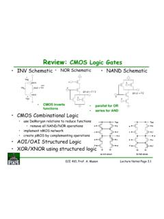
Review: CMOS Logic Gates - Michigan State University
www.egr.msu.edu• Physical structure of CMOS devices and circuits – pMOS and nMOS devices in a CMOS process – n-well CMOS process, device isolation • Fabrication processes • Physical design (layout) – layout of basic digital gates, masking layers, design rules ss–LecOOCoS pr – planning complex layouts (Euler Graph and Stick Diagram) Part I ...
Sample & Hold Circuits - Pennsylvania State University
www.cse.psu.eduRudy van de Plassche, “CMOS Integrated Analog-to-Digital and Digital-to-Analog Converters- 2nd Edition,” Kluwer Academic Publishers, 2003.Kluwer Academic Publishers, 2003. B. Razavi, “Principles of Data Conversion System Design,” IEEE Press, 1995. 3/14/2011 Insoo Kim
CMOS Analog Circuit Design
picture.iczhiku.comanalog–digital and digital–analog converters is presented. These converters allow high reso-lution and are very compatible with CMOS technology. Five appendices cover the topics of circuit analysis methods for CMOS analog circuits, integrated circuit layout, CMOS device characterization (this is essentially Chapter 4 of the

Omni ision Preliminary Datasheet Advanced Information
web.mit.eduOV7670/OV7171 CMOS VGA (640x480) CAMERACHIPTM Sensor Omni ision ® with OmniPixel® Technology General Description The OV7670/OV7171 CAMERACHIPTM image sensor is a low voltage CMOS device that provides the full functionality of a single-chip VGA camera and image processor in a small footprint package.

AD9850 CMOS, 125 MHz Complete DDS Synthesizer Data …
www.analog.coma cmos, 125 mhz complete dds synthesizer ad9850 functional block diagram clock out clock out analog in analog out dac rset +vs gnd comparator phase and control words serial load 32-bit tuning word high speed dds frequency/phase data register parallel data input register ad9850 10-bit dac ref clock in master reset word load clock frequency ...