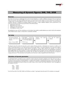
Transcription of Sample & Hold Circuits - Pennsylvania State University
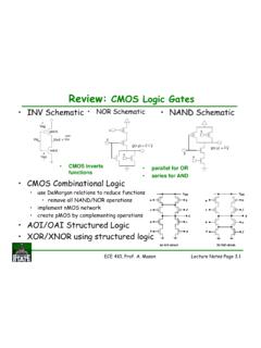
1 CSE 577 Spring2011 Sample & hold CircuitsSample & hold CircuitsCSE 577 Spring 2011 Sample & hold Circuits Sample & hold Circuits Insoo Kim, Kyusun ChoiMixed Signal CHIP Design of Computer Science & EngineeringDepartment of Computer Science & EngineeringThe Pennsylvania State UniversityBasic Sample and hold circuit ConfigurationBasic Sample and hold circuit Configuration Concept MOSFET S&H CircuitInsoo Kim3/14/2011 Design Issues of cmos S&HDesign Issues of cmos S&H Sampling Moment Distortion Finite Clock rising/falling time results in distortionriseclockstVat2= Clock Feed-through Overlap cap. of MOS Switch creates an sampling error during clock transition time MOS Switch Charge Injection Some charge in the MOS channel flow to Source and Drain, then result in an error. holdThGSoxQVVVCQ = = ),(Insoo Kim3/14/2011 HholdThGSoxCQ),(Solutions for Reducing Sampling DistortionSolutions for Reducing Sampling Distortion Differential S&H circuit Sample Clock Bootstrapping Sampling distortion can be reduced by increasing clock amplitudeInsoo Kim3/14/2011 Sample Clock Bootstrap Circuits (I) Sample Clock Bootstrap Circuits (I) Basic clock bootstrap circuitBooted ClockClockSimulation ResultInsoo Kim3/14/2011 Sample Clock Bootstrap Circuits (II) Sample Clock Bootstrap Circuits (II) Differential sampling clock bootstrap circuitDifferential Sampling Booted ClockSingle sampling booted ClockClockSimulation ResultInsoo Kim3/14/2011 Signal Dependent Clock Bootstrapping (I)Signal Dependent Clock Bootstrapping (I)
2 The problem of clock bootstrap circuit Vgs of MOS switch can vary according to the input voltage level Ron of MOS Switch also vary Ron of MOS Switch also vary It can cause an error in holding voltage Signal Dependent clock bootstrap circuitInsoo Kim3/14/2011 Signal Dependent Clock Bootstrapping (II)Signal Dependent Clock Bootstrapping (II) Modified CircuitInsoo Kim3/14/2011 Low Signal FeedLow Signal Feed--through Switchthrough Switch SchematicOffset: 30 mVOffset: 30 mVSimulation ResultInsoo Kim3/14/2011 Charge injection Compensation Switch (I)Charge injection Compensation Switch (I)Offset: mVVinVoutSimulation ResultInsoo Kim3/14/2011 Charge injection Compensation Switch (II)Charge injection Compensation Switch (II)Offset: mVVinVoutOffset: mVSimulation ResultInsoo Kim3/14/2011 Actual Implementation S&HActual Implementation S&HActual Implementation S&H Actual Implementation S&H CircuitsCircuitsDouble Buffered S&H ConfigurationDouble Buffered S&H ConfigurationAdvantages:Advantages:- Obtain a low droop rate during holding mode- Stability is determined by the stabilities of OP AmpsDisadvantages:- OP Amps offset can constrain the accuracy of SHAI nsoo Kim3/14/2011 Double Buffered S&H circuit with cmos SwitchDouble Buffered S&H circuit with cmos Switch SchematicInsoo Kim3/14/2011 Double Buffered S&H circuit with cmos SwitchDouble Buffered S&H circuit with cmos Switch Simulation ResultInputOutputInputVSS ( )VDD ( )Insoo Kim3/14/2011 Feedback Improved S&H CircuitFeedback Improved S&H CircuitAdvantages:Off t f MtthdblbffdSHA-Offset free More accurate than double buffered SHAD isadvantages.
3 Common Mode Rejection of the Input OP amp must be high-Common Mode Rejection of the Input OP amp must be high- Special Care must be taken to obtain stability of SHA - Needs a special circuitry to stabilize the input amplifier during the holding modeInsoo Kim3/14/2011during the holding mode(cont d) Feedback Improved S&H circuit (cont d) Feedback Improved S&H CircuitSimple stabilization circuit for input amplifierInsoo Kim3/14/2011(cont d) Feedback Improved S&H circuit (cont d) Feedback Improved S&H CircuitFeedback improved S&H w/o input amp stabilizationinput amp stabilizationFdbkidS&HFeedback improved S&H with input amp stabilizationSimulation ResultInsoo Kim3/14/2011 Simulation ResultIntegrating S&H CircuitIntegrating S&H CircuitAdvantages:- Switching moment and charge feed-through can be tlldllcontrolled very wellDisadvantages:-Common Mode Rejection of the Input OP amp must be high-Common Mode Rejection of the Input OP amp must be high- Special Care must be taken to obtain stability of SHA - Needs a special circuitry to stabilize the input amplifier during the holding modeInsoo Kim3/14/2011during the holding modeS&H circuit using Miller circuit using Miller Kim3/14/2011 Switched Capacitor S&H CircuitSwitched Capacitor S&H circuit Basic Configuration Common implementation for pipelined ADCsInsoo Kim3/14/2011 ReferencesReferences Rudy van de Plassche, cmos Integrated Analog-to- digital and digital -to-Analog Converters- 2ndEdition, Kluwer Academic Publishers, Academic Publishers, 2003.
4 B. Razavi, Principles of Data Conversion System Design, IEEE Press, Kim3/14/2011