Transcription of CDCVF2505 3.3-V Clock Phase Lock-Loop Clock Driver ...
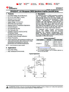
1 Product Sample & Technical Tools & Support &. Folder Buy Documents Software Community CDCVF2505 . SCAS640G JULY 2000 REVISED AUGUST 2016. CDCVF2505 Clock Phase -Lock Loop Clock Driver 1 Features 3 Description 1 Phase -Lock Loop Clock Driver for Synchronous The CDCVF2505 is a high-performance, low-skew, DRAM and General-Purpose Applications low-jitter, Phase -lock loop (PLL) Clock Driver . This device uses a PLL to precisely align the output clocks Spread Spectrum Clock Compatible (1Y[0-3] and CLKOUT) to the input Clock signal Operating Frequency: 24 MHz to 200 MHz (CLKIN) in both frequency and Phase . The Low Jitter (Cycle-to-Cycle): < |150 ps| CDCVF2505 operates at V and also provides (Over 66 MHz to 200 MHz Range) integrated series-damping resistors that make it ideal for driving point-to-point loads.
2 Distributes One Clock Input to One Bank of Five Outputs (CLKOUT Used to Tune the Input-Output One bank of five outputs provides low-skew, low-jitter Delay) copies of CLKIN. Output duty cycles are adjusted to 50 percent, independent of duty cycle at CLKIN. The Three-States Outputs When There Is No Input device automatically goes into power-down mode Clock when no input signal is applied to CLKIN. Operates From Single Supply The loop filter for the PLLs is included on-chip. This Available in 8-Pin TSSOP and 8-Pin SOIC minimizes the component count, space, and cost. Packages The CDCVF2505 is characterized for operation from Consumes Less Than 100 mA (Typical) in Power- 40 C to 85 C. Down Mode Internal Feedback Loop Is Used to Synchronize Device Information(1). the Outputs to the Input Clock PART NUMBER PACKAGE BODY SIZE (NOM).
3 25- On-Chip Series Damping Resistors SOIC (8) mm mm CDCVF2505 . Integrated RC PLL Loop Filter Eliminates the TSSOP (8) mm mm Need for External Components (1) For all available packages, see the orderable addendum at the end of the data sheet. 2 Applications Functional Block Diagram Synchronous DRAMs Industrial Applications 8. General-Purpose Zero-Delay Clock Buffers CLKIN. 1 PLL. 25 W. CLKOUT. 3. 1Y0. 25 W. 2. 1Y1. Power Down 25 W. 5. 1Y2. 25 W. 7. 1Y3. 25 W. Edge Detect 3-State Typical <10 MHz B0246-01. Copyright 2016, Texas Instruments Incorporated 1. An IMPORTANT NOTICE at the end of this data sheet addresses availability, warranty, changes, use in safety-critical applications, intellectual property matters and other important disclaimers. PRODUCTION DATA. CDCVF2505 . SCAS640G JULY 2000 REVISED AUGUST 2016 Table of Contents 1 Features.
4 1 Functional Block Diagram .. 8. 2 Applications .. 1 Feature 8. 3 Description .. 1 Device Functional 9. 4 Revision 2 10 Application and 10. Application 10. 5 Description (continued).. 3. Typical Application .. 10. 6 Pin Configuration and Functions .. 3. 11 Power Supply Recommendations .. 12. 7 4. Absolute Maximum Ratings .. 4 12 12. Layout Guidelines .. 12. ESD 4. Layout Example .. 12. Recommended Operating 4. Thermal Information .. 4 13 Device and Documentation Support .. 13. Electrical 5 Documentation Support .. 13. Timing Requirements .. 5 Receiving Notification of Documentation Updates 13. Switching Characteristics .. 6 Community 13. Typical Characteristics .. 6 Trademarks .. 13. Electrostatic Discharge Caution .. 13. 8 Parameter Measurement Information .. 7. Glossary .. 13. 9 Detailed Description.
5 8. Overview .. 8 14 Mechanical, Packaging, and Orderable Information .. 13. 4 Revision History NOTE: Page numbers for previous revisions may differ from page numbers in the current version. Changes from Revision F (February 2012) to Revision G Page Added ESD Ratings table, Feature Description section, Device Functional Modes, Application and Implementation section, Power Supply Recommendations section, Layout section, Device and Documentation Support section, and Mechanical, Packaging, and Orderable Information section .. 1. Changed R JA value for D package from : to C/W .. 4. Changed R JA value for PW package from C/W : to 4. Updated values in the Thermal Information table to align with JEDEC standards.. 4. 2 Submit Documentation Feedback Copyright 2000 2016, Texas Instruments Incorporated Product Folder Links: CDCVF2505 .
6 CDCVF2505 . SCAS640G JULY 2000 REVISED AUGUST 2016. 5 Description (continued). Because it is based on the PLL circuitry, the CDCVF2505 requires a stabilization time to achieve Phase lock of the feedback signal to the reference signal. This stabilization is required following power up and application of a fixed-frequency, fixed- Phase signal at CLKIN, and following any changes to the PLL reference. 6 Pin Configuration and Functions D or PW Package 8-Pin SOIC or TSSOP. Top View CLKIN 1 8 CLKOUT. 1Y1 2 7 1Y3. 1Y0 3 6 GND 4 5 1Y2. Not to scale Pin Functions PIN. TYPE (1) DESCRIPTION. NAME NO. Clock outputs. These outputs are low-skew copies of CLKIN. Each output has an integrated 1Y[0 3] 2, 3, 5, 7 O. 25- series damping resistor. Clock input. CLKIN provides the Clock signal to be distributed by the CDCVF2505 Clock Driver .
7 CLKIN is used to provide the reference signal to the integrated PLL that generates the CLKIN 1 I Clock output signals. CLKIN must have a fixed frequency and fixed Phase for the PLL to obtain Phase lock. Once the circuit is powered up and a valid signal is applied, a stabilization time (100 s) is required for the PLL to Phase lock the feedback signal to CLKIN. Feedback output. CLKOUT completes the internal feedback loop of the PLL. This connection CLKOUT 8 O is made inside the chip and an external feedback loop should NOT be connected. CLKOUT. can be loaded with a capacitor to achieve zero delay between CLKIN and the Y outputs. GND 4 P Ground 6 P supply (1) I = Input, O = Output, and P = Power Copyright 2000 2016, Texas Instruments Incorporated Submit Documentation Feedback 3. Product Folder Links: CDCVF2505 .
8 CDCVF2505 . SCAS640G JULY 2000 REVISED AUGUST 2016 7 Specifications Absolute Maximum Ratings over operating free-air temperature range (unless otherwise noted) (1). MIN MAX UNIT. VDD Supply voltage V. (2) (3). VI Input voltage VDD + V. VO Output voltage (2) (3) VDD + V. IIK Input clamp current (VI < 0 or VI > VDD) 50 mA. IOK Output clamp current (VO < 0 or VO > VDD) 50 mA. IO Continuous total output current (VO = 0 to VDD) 50 mA. Tstg Storage temperature 65 150 C. (1) Stresses beyond those listed under Absolute Maximum Ratings may cause permanent damage to the device. These are stress ratings only, and functional operation of the device at these or any other conditions beyond those indicated under Recommended Operating Conditions is not implied. Exposure to absolute-maximum-rated conditions for extended periods may affect device reliability.
9 (2) The input and output negative-voltage ratings may be exceeded if the input and output clamp-current ratings are observed. (3) This value is limited to V maximum. ESD Ratings VALUE UNIT. (1). Human-body model (HBM), per ANSI/ESDA/JEDEC JS-001 2000. V(ESD) Electrostatic discharge Charged-device model (CDM), per JEDEC specification JESD22-C101 (2) 1000 V. Machine model (MM) 300. (1) JEDEC document JEP155 states that 500-V HBM allows safe manufacturing with a standard ESD control process. (2) JEDEC document JEP157 states that 250-V CDM allows safe manufacturing with a standard ESD control process. Recommended Operating Conditions over operating free-air temperature range (unless otherwise noted). MIN NOM MAX UNIT. VDD Supply voltage 3 V. VIH High-level input voltage VDD V. VIL Low-level input voltage VDD V.
10 VI Input voltage 0 VDD V. IOH High-level output current 12 mA. IOL Low-level output current 12 mA. TA Operating free-air temperature 40 85 C. Thermal Information CDCVF2505 . (1). THERMAL METRIC D (SOIC) PW (TSSOP) UNIT. 8 PINS 8 PINS. R JA Junction-to-ambient thermal resistance (2) C/W. R JC(top) Junction-to-case (top) thermal resistance C/W. R JB Junction-to-board thermal resistance C/W. JT Junction-to-top characterization parameter C/W. JB Junction-to-board characterization parameter C/W. R JC(bot) Junction-to-case (bottom) thermal resistance C/W. (1) For more information about traditional and new thermal metrics, see the Semiconductor and IC Package Thermal Metrics application report. (2) The package thermal impedance is calculated in accordance with JESD 51. 4 Submit Documentation Feedback Copyright 2000 2016, Texas Instruments Incorporated Product Folder Links: CDCVF2505 .
