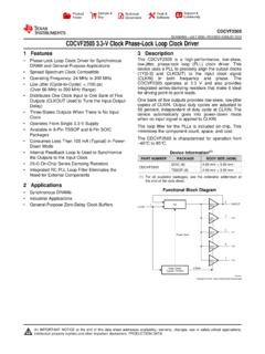
Transcription of HIGH ISOLATION VOLTAGE AC INPUT RESPONSE TYPE …
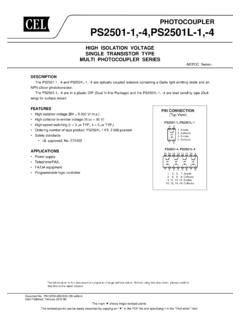
1 The mark <R> shows major revised points. The revised points can be easily searched by copying an "<R>" in the PDF file and specifying it in the "Find what:" field. PHOTOCOUPLERPS2505-1,-4,PS2505L-1,-4 high ISOLATION VOLTAGE AC INPUT RESPONSE TYPE MULTI PHOTOCOUPLER SERIES NEPOC Series Document No. PN10228EJ03V0DS (3rd edition) Date Published September 2009 NS PIN CONNECTION(Top View)PS2505-1, PS2505L-1PS2505-4, PS2505L-412431. Anode, Cathode2. Cathode, Anode3. Emitter4. Collector 1, 3, 5, 7. Anode, Cathode 2, 4, 6, 8. Cathode, Anode 9, 11, 13, 15. Emitter10, 12, 14, 16. Collector1234567816 15 14 13 12 11 10 9 DESCRIPTION The PS2505-1, -4 and PS2505L-1, -4 are optically coupled isolators containing GaAs light emitting diodes and an NPN silicon phototransistor. The PS2505-1, -4 are in a plastic DIP (Dual In-line Package) and the PS2505L-1, -4 are lead bending type (Gull-wing) for surface mount.
2 FEATURES AC INPUT RESPONSE high ISOLATION VOLTAGE (BV = 5 000 ) high collector to emitter VOLTAGE (VCEO = 80 V) high -speed switching (tr = 3 s TYP., tf = 5 s TYP.) Ordering number of tape product: PS2505L-1-F3: 2 000 pcs/reel Safety standards UL approved: No. E72422 APPLICATIONS Power supply Telephone/FAX. FA/OA equipment Programmable logic controller<R> <R>Data Sheet PN10228EJ03V0DS 2PS2505-1,-4,PS2505L-1,-4 PACKAGE DIMENSIONS (UNIT : mm) DIP Type M0 to 15 + to 15 + Bending Type + + + + CONSTRUCTION ParameterUnit (MIN.)Air Distance 7 mm Outer Creepage Distance 7 mm Inner Creepage Distance mm ISOLATION Thickness mm <R> <R>Data Sheet PN10228EJ03V0DS 3PS2505-1,-4,PS2505L-1,-4 MARKING EXAMPLE 2505NJ931PS2505-4NJ931 JPS2505-1PS2505-4 Assembly LotWeek AssembledYear Assembled(Last 1 Digit)In-house CodeCTR Rank CodeNo.
3 1 pinMarkPackageNew PKGMade in JapanMade in TaiwanNo. 1 pinMarkNJWeek AssembledYear Assembled(Last 1 Digit)In-house CodeCTR Rank CodePackageNew PKGMade in Japan931N931 Country AssembledType NumberAssembly LotJJK<R>Data Sheet PN10228EJ03V0DS 4PS2505-1,-4,PS2505L-1,-4 ORDERING INFORMATION Part Number Order Number Solder Plating Specification Packing Style Safety Standard Approval Application Part Number*1 PS2505-1 PS2505-1-A Pb-Free Magazine case 100 pcs Standard products PS2505-1 PS2505L-1 PS2505L-1-A (UL Approved) PS2505L-1-F3 PS2505L-1-F3-A Embossed Tape 2 000 pcs/reel PS2505-4 PS2505-4-A Magazine case 20 pcs PS2505-4 PS2505L-4 PS2505L-4-A *1 For the application of the Safety Standard, following part number should be MAXIMUM RATINGS (TA = 25 C, unless otherwise specified) RatingsParameterSymbol PS2505-1, PS2505L-1 PS2505-4, PS2505L-4 Unit Diode Forward Current (DC)
4 IF 80mA/chPower Dissipation Derating PD/ mW/ C Power DissipationPD150120 mW/chPeak Forward Current*1 IFP 1A/chTransistor Collector to Emitter VOLTAGE VCEO80 VEmitter to Collector VOLTAGE VECO7 VCollector CurrentIC50mA/chPower Dissipation Derating PC/ mW/ C Power DissipationPC150120 mW/chIsolation VOLTAGE *2BV 5 000 Ambient Temperature TA 55 to +100 C Storage Temperature Tstg 55 to +150 C *1 PW = 100 s, Duty Cycle = 1%*2 AC VOLTAGE for 1 minute at TA = 25 C, RH = 60% between INPUT and outputPins 1-2 shorted together, 3-4 shorted together (PS2505-1, PS2505L-1).Pins 1-8 shorted together, 9-16 shorted together (PS2505-4, PS2505L-4). <R>Data Sheet PN10228EJ03V0DS 5PS2505-1,-4,PS2505L-1,-4 ELECTRICAL CHARACTERISTICS (TA = 25 C) ParameterSymbolConditionsMIN.
5 TYP. MAX. UnitDiode Forward VOLTAGE VF IF = 10 mA V Terminal Capacitance Ct V = 0 V, f = MHz 100 pF Transistor Collector to Emitter Dark Current ICEO VCE = 80 V, IF = 0 mA 100 nA Coupled Current Transfer Ratio (IC/IF) CTR IF = 5 mA, VCE = 5 V 80 300 600 % CTR Ratio*1 CTR1/CTR2 IF = 5 mA, VCE = 5 V Collector Saturation VOLTAGE VCE (sat) IF = 10 mA, IC = 2 mA V ISOLATION Resistance RI-O VI-O = kVDC1011 ISOLATION CapacitanceCI-OV = 0 V, f = MHz pF Rise T ime*2tr VCC = 10 V, IC = 2 mA, RL = 100 3 s Fall Time*2tf5 *1 CTR1 = IC1/IF1, CTR2 = IC2/IF2IF1IF2IC1IC2 VCE*2 Test circuit for switching timeVCCVOUTRL = 100 50 PW = 100 sDuty Cycle = 1/10 IFPulse InputData Sheet PN10228EJ03V0DS 6PS2505-1,-4,PS2505L-1,-4 TYPICAL CHARACTERISTICS (TA = 25 C, unless otherwise specified) mW/ mW/ C150100502550100125150010 0001001 0001001017550250 25 50 VCE = 80 mW/ mW/ C20 mA50 mA2 mA IF = 1 mA5 mA40 V24 V10 V5 VPS2505-1PS2505L-1PS2505-4PS2505L-4PS250 5-1PS2505L-1PS2505-4PS2505L-4 40 80 600 C 25 C 55 C+60 C+25 CTA = +100 CDiode Power Dissipation PD (mW)
6 Transistor Power Dissipation PC (mW)Ambient Temperature TA ( C)Forward Current IF (mA)Forward VOLTAGE VF (V)Collector to Emitter Dark Current ICEO (nA)Collector Saturation VOLTAGE VCE (sat) (V)Ambient Temperature TA ( C)Ambient Temperature TA ( C)DIODE POWER DISSIPATION TEMPERATURETRANSISTOR POWER DISSIPATIONvs. AMBIENT TEMPERATUREFORWARD CURRENT VOLTAGECOLLECTOR TO EMITTER DARKCURRENT vs. AMBIENT TEMPERATURECOLLECTOR CURRENT SATURATION VOLTAGEC ollector Current IC (mA)Forward Current IF (mA)Forward VOLTAGE VF (V)FORWARD CURRENT VOLTAGE75 Remark The graphs indicate nominal characteristics. <R>Data Sheet PN10228EJ03V0DS 7PS2505-1,-4,PS2505L-1, k5 k1 k50010050101 000100101100 k50 k10 k5 k1 k5001000 5 10 15 12510 2050 100 200 500IC = 2 mA,VCC = 10 V,CTR = 290%tftrtdtsIF = 5 mA,VCC = 5 V,CTR = 290%tstdtrtfIF = 5 mA,VCE = 5 V100 300 RL = 1 k 70260504030201004681020 mAIF = 5 mA10 mA50 mACollector Current IC (mA)Collector to Emitter VOLTAGE VCE (V)COLLECTOR CURRENT TO EMITTER VOLTAGEN ormalized to TA = 25 C,IF = 5 mA, VCE = 5 VForward Current IF (mA)Ambient Temperature TA ( C)Load Resistance RL ( )Frequency f (kHz)Normalized Current Transfer Ratio CTRC urrent Transfer Ratio CTR (%)Normalized Gain GVLoad Resistance RL ( )Switching Time t ( s) NORMALIZED CURRENT TRANSFERRATIO vs.
7 AMBIENT TEMPERATURECURRENT TRANSFER RATIO CURRENTSWITCHING TIME RESISTANCESWITCHING TIME RESISTANCEFREQUENCY RESPONSES witching Time t ( s) ABCDVCE = 5 VRemark The graphs indicate nominal characteristics. Data Sheet PN10228EJ03V0DS 8PS2505-1,-4,PS2505L-1,-4TA = 25 CTA = 60 (Hr)CTR (Relative Value)LONG TERM CTR DEGRADATIONIF = 5 mA Remark The graph indicates nominal characteristics. Data Sheet PN10228EJ03V0DS 9PS2505-1,-4,PS2505L-1,-4 TAPING SPECIFICATIONS (UNIT : mm) Tape DirectionOutline and Dimensions (Tape)Outline and Dimensions (Reel) + 0 Packing: 2 000 330 to edge of <R>Data Sheet PN10228EJ03V0DS 10PS2505-1,-4,PS2505L-1,-4 NOTES ON HANDLING soldering conditions(1) Infrared reflow soldering Peak reflow temperature260 C or below (package surface temperature) Time of peak reflow temperature10 seconds or less Time of temperature higher than 220 C60 seconds or less Time to preheat temperature from 120 to 180 C 120 30 s Number of reflowsThree FluxRosin flux containing small amount of chlorine (The flux with a maximum chlorine content of Wt% is recommended.)
8 120 30 s(preheating)220 C180 CPackage Surface Temperature T ( C)Time (s)Recommended Temperature Profile of Infrared Reflow(heating)to 10 sto 60 s260 C C(2) Wave soldering Temperature260 C or below (molten solder temperature) Time10 seconds or less Preheating conditions 120 C or below (package surface temperature) Number of timesOne (Allowed to be dipped in solder including plastic mold portion.) FluxRosin flux containing small amount of chlorine (The flux with a maximum chlorine content of Wt% is recommended.) (3) Soldering by soldering iron Peak temperature (lead part temperature) 350 C or below Time (each pins)3 seconds or less FluxRosin flux containing small amount of chlorine (The flux with a maximum chlorine content of Wt% is recommended.) (a)Soldering of leads should be made at the point to mm from the root of the lead.(b)Please be sure that the temperature of the package would not be heated over 100 Sheet PN10228EJ03V0DS 11PS2505-1,-4,PS2505L-1,-4(4) Cautions FluxesAvoid removing the residual flux with freon-based and chlorine-based cleaning Cautions regarding noiseBe aware that when VOLTAGE is applied suddenly between the photocoupler s INPUT and output or betweencollector-emitters at startup, the output transistor may enter the on state, even if the VOLTAGE is within the absolutemaximum Measurement conditions of current transfer ratios (CTR), which differ according to photocouplerCheck the setting values before use, since the forward current conditions at CTR measurement differ accordingto using products other than at the specified forward current, the characteristics curves may differ from the standard curves due to CTR value variations or the like.
9 This tendency may sometimes be obvious, especially below IF = 1 mA. Therefore, check the characteristics under the actual operating conditions and thoroughly take variations or the like into consideration before use. USAGE CAUTIONS against static electricity when storage at a high temperature and high ,-4,PS2505L-1,-4 Caution GaAs Products This product uses gallium arsenide (GaAs). GaAs vapor and powder are hazardous to human health if inhaled or ingested, so please observe the following points. Follow related laws and ordinances when disposing of the product. If there are no applicable lawsand/or ordinances, dispose of the product as recommended Commission a disposal company able to (with a license to) collect, transport and dispose ofmaterials that contain arsenic and other such industrial waste Exclude the product from general industrial waste and household garbage, and ensure that theproduct is controlled (as industrial waste subject to special control) up until final disposal.
10 Do not burn, destroy, cut, crush, or chemically dissolve the product. Do not lick the product or in any way allow it to enter the of circuits, software and other related information in this document are provided only to illustrate the operation of semiconductor products andapplication examples. You are fully responsible for the incorporation of these circuits, software, and information in the design of your equipment. CaliforniaEastern Laboratories and Renesas Electronics assumes no responsibility for any losses incurred by you or third parties arising from the use of these circuits, software, or Eastern Laboratories has used reasonable care in preparing the information included in this document, but California Eastern Laboratories doesnot warrant that such information is error free. California Eastern Laboratories and Renesas Electronics assumes no liability whatsoever for any damagesincurred by you resulting from errors in or omissions from the information included Eastern Laboratories and Renesas Electronics do not assume any liability for infringement of patents, copyrights, or other intellectual propertyrights of third parties by or arising from the use of Renesas Electronics products or technical information described in this document.