Transcription of CHAPTER 1 OUTLINE - ce L
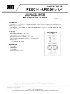
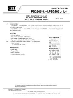
1 PHOTOCOUPLERPS2805-1,PS2805-4 HIGH ISOLATION VOLTAGE AC INPUT RESPONSE TYPE SSOP PHOTOCOUPLER NEPOC Series The mark shows major revised points. Document No. PN10253EJ03V0DS (3rd edition) Date Published March 2006 CP(K) DESCRIPTION The PS2805-1 and PS2805-4 are optically coupled isolators containing GaAs light emitting diodes and an NPN silicon phototransistor in a plastic SSOP for high density applications. This package has shield effect to cut off ambient light. FEATURES High isolation voltage (BV = 2 500 ) Small and thin package (4,16-pin SSOP, Pin pitch mm) High collector to emitter voltage (VCEO = 80 V) AC input response High-speed switching (tr = 3 s TYP.)
2 , tf = 5 s TYP.) Ordering number of tape product: PS2805-1-F3, F4, PS2805-4-F3, F4 Pb-Free product Safety standards: PS2805-1, -4 UL approved: File No. E72422 BSI approved: No. 8188, 8189 CSA approved: File No. CA 101391 DIN EN60747-5-2 (VDE0884 Part2) approved (Option) APPLICATIONS Programmable logic controllers Measuring instruments Hybrid IC NEC Compound Semiconductor Devices, Ltd. 1991, 2006 1. Anode, Cathode2. Cathode, Anode3. Emitter4. Collector4312 Anode, CathodeCathode, AnodeEmitterCollector1. 3. 5. 7. 2. 4. 6. 11. 13. 12. 14. 15 14 13 12 11 10 9PS2805-4PS2805-1(Top View)PIN CONNECTIONData Sheet PN10253EJ03V0DS 2 PS2805-1,PS2805-4 PACKAGE DIMENSIONS (UNIT: mm) + + + + MARKING EXAMPLE 5401 Assembly Lot 4 01 Week AssembledYear Assembled(Last 1 Digit)Last number of type No.
3 : 5PS2805-1 Country AssembledAssembly LotNo. 1 pinMarkPS2805-4PS2805-4NL401 Type Number*1401 Year Assembled(Last 1 Digit)LNRank CodeIn-house Code(L: Pb-Free)Week Assembled*1 : Pb-Free Data Sheet PN10253EJ03V0DS 3 PS2805-1,PS2805-4 ORDERING INFORMATION Part Number Order Number Solder Plating Specification Packing Style Safety Standard Approval Application Part Number*1PS2805-1 PS2805-1-A Pb-Free 50 pcs (Tape 50 pcs cut) Standard products PS2805-1 PS2805-1-F3 PS2805-1-F3-A Embossed Tape 3 500 pcs/reel (UL, BSI, CSA PS2805-1-F4 PS2805-1-F4-A approved) PS2805-1-V PS2805-1-V-A 50 pcs (Tape 50 pcs cut)
4 DIN EN60747-5-2 PS2805-1-V-F3 PS2805-1-V-F3-A Embossed Tape 3 500 pcs/reel (VDE0884 Part2) PS2805-1-V-F4 PS2805-1-V-F4-A Approved (Option) PS2805-4 PS2805-4-A Magazine Case 45 pcs Standard products PS2805-4 PS2805-4-F3 PS2805-4-F3-A Embossed Tape 2 500 pcs/reel (UL, BSI, CSA PS2805-4-F4 PS2805-4-F4-A approved)
5 PS2805-4-V PS2805-4-V-A Magazine Case 45 pcs DIN EN60747-5-2 PS2805-4-V-F3 PS2805-4-V-F3-A Embossed Tape 2 500 pcs/reel (VDE0884 Part2) PS2805-4-V-F4 PS2805-4-V-F4-A Approved (Option) *1 For the application of the Safety Standard, following part number should be used. Data Sheet PN10253EJ03V0DS 4 PS2805-1,PS2805-4 ABSOLUTE MAXIMUM RATINGS (Unless otherwise specified, TA = 25 C) Parameter Symbol Ratings Unit PS2805-1 PS2805-4 Diode Forward Current (DC)
6 IF 50 mA/ch Power Dissipation Derating PD/ C mW/ C Power Dissipation PD 60 80 mW/ch Peak Forward Current *1 IFP 1 A/ch Transistor Collector to Emitter Voltage VCEO 80 V Emitter to Collector Voltage VECO 6 V Collector Current IC 50 mA/ch Power Dissipation Derating PC/ C mW/ C Power Dissipation PC 120 mW/ch Isolation Voltage *2 BV 2 500 Operating Ambient
7 Temperature TA 55 to +100 C Storage Temperature Tstg 55 to +150 C *1 PW = 100 s, Duty Cycle = 1% *2 AC voltage for 1 minute at TA = 25 C, RH = 60% between input and output. Pins 1-2 shorted together, 3-4 shorted together (PS2805-1). Pins 1-8 shorted together, 9-16 shorted together (PS2805-4). Data Sheet PN10253EJ03V0DS 5 PS2805-1,PS2805-4 ELECTRICAL characteristics (TA = 25 C) Parameter Symbol Conditions MIN. TYP. MAX. Unit Diode Forward Voltage VF IF = 5 mA V Terminal Capacitance Ct V = 0 V, f = MHz 30 pF Transistor Collector to Emitter Dark Current ICEO VCE = 80 V, IF = 0 mA 100 nA Coupled Current Transfer Ratio (IC/IF) CTR IF = 5 mA, VCE = 5 V 80 600 % CTR Ratio *1 CTR1/ CTR2 IF = 5 mA, VCE = 5 V Collector Saturation Voltage VCE(sat)
8 IF = 10 mA, IC = 2 mA V Isolation Resistance RI-O VI-O = kVDC 1011 Isolation Capacitance CI-O V = 0 V, f = MHz pF Rise Time *2 tr VCC = 5 V, IC = 2 mA, RL = 100 3 s Fall Time *2 tf 5 *1 CTR1 = IC1/IF1, CTR2 = IC2/IF2 IC1IC2 VCEIF1IF2 *2 Test circuit for switching time IFPulse InputVCC50 RL = 100 VOUTPW = 100 sDuty Cycle = 1/10 Data Sheet PN10253EJ03V0DS 6 PS2805-1,PS2805-4 TYPICAL characteristics (Unless otherwise specified, TA = 25 C) mW/ mW/ C255075100100806040200 Ambient Temperature TA ( C) Diode Power Dissipation PD (mW)DIODE POWER DISSIPATION mW/ CAmbient Temperature TA ( C)Transistor Power Dissipation PC (mW)TRANSISTOR POWER DISSIPATIONvs.
9 AMBIENT Voltage VF (V)Forward Current IF (mA)FORWARD CURRENT VOLTAGETA = +100 C+60 C+25 C0 C 25 C 55 C10010 0001 000101 50 250100255075 Collector to Emitter Dark Current ICEO (nA)Ambient Temperature TA ( C)COLLECTOR TO EMITTER DARKCURRENT vs. AMBIENT TEMPERATUREVCE = 80 V40 V24 V10 V5 V 40 80 600 20402060 Forward Current IF (mA)Forward Voltage VF (V)FORWARD CURRENT VOLTAGE1 mAIF = 50 mA20 mA10 mA5 mA2 Saturation Voltage VCE(sat) (V)Collector Current IC (mA)COLLECTOR CURRENT SATURATION VOLTAGE Remark The graphs indicate nominal characteristics . Data Sheet PN10253EJ03V0DS 7 PS2805-1,PS2805-4 Normalized to TA = 25 C,IF = 5 mA, VCE = 5 V 500100 Temperature TA ( C)Normalized Current Transfer Ratio CTRNORMALIZED CURRENT TRANSFERRATIO vs.
10 AMBIENT TEMPERATURE tftstrtdVCC = 5 V,IC = 2 mA,CTR = 236% Resistance RL (k )Switching Time t ( s) SWITCHING TIME RESISTANCEVCC = 5 V,IF = 5 mA,CTR = 236% 000 Load Resistance RL (k )Switching Time t ( s) SWITCHING TIME RESISTANCE IF = 5 mA,TA = 25 CIF = 20 mA,TA = 25 CIF = 5 mA,TA = 60 CLONG TERM CTR DEGRADATIONTime (Hr)CTR (Relative Value) to Emitter Voltage VCE (V)Collector Current IC (mA)COLLECTOR CURRENT vs. COLLECTOR TO EMITTER VOLTAGE5 mAIF = 50 mA10 mA20 Current IF (mA)Current Transfer Ratio CTR (%)CURRENT TRANSFER RATIO CURRENTVCE = 5 V,n = 3 Sample ABC Remark The graphs indicate nominal characteristics . Data Sheet PN10253EJ03V0DS 8 PS2805-1,PS2805-4 FREQUENCY RESPONSEF requency f (kHz)Normalized Gain Gv 10 20 150 205001550 100200IF = 5 mA,VCE = 5 VRL = 1 k 100 300 Remark The graph indicates nominal characteristics .
