Transcription of CHAPTER 1 OUTLINE - ce L
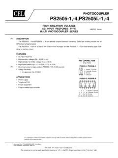
1 PHOTOCOUPLERPS2501-1,-4,PS2501L-1,-4 HIGH ISOLATION VOLTAGE SINGLE TRANSISTOR TYPE MULTI PHOTOCOUPLER SERIES NEPOC Series Document No. PN10225EJ05V0DS (5th edition) Date Published February 2010 NS DESCRIPTION The ps2501 -1, -4 and PS2501L-1, -4 are optically coupled isolators containing a GaAs light emitting diode and an NPN silicon phototransistor. The ps2501 -1, -4 are in a plastic DIP (Dual In-line Package) and the PS2501L-1, -4 are lead bending type (Gull-wing) for surface mount. FEATURES ps2501 -1, PS2501L-11. Anode2. Cathode3. Emitter4. Collector1243PS2501-4, PS2501L-41234567816 15 14 13 12 11 10 9 1, 3, 5, 7. Anode 2, 4, 6, 8. Cathode 9, 11, 13, 15. Emitter10, 12, 14, 16.
2 Collector(Top View)PIN CONNECTION High isolation voltage (BV = 5 000 ) High collector to emitter voltage (VCEO = 80 V) High-speed switching (tr = 3 s TYP., tf = 5 s TYP.) Ordering number of tape product: PS2501L-1-F3: 2 000 pcs/reel Safety standards UL approved: No. E72422 APPLICATIONS Power supply Telephone/FAX. FA/OA equipment Programmable logic controller The mark shows major revised points. The revised points can be easily searched by copying an " " in the PDF file and specifying it in the "Find what:" field. ps2501 -1,-4,PS2501L-1,-4 PACKAGE DIMENSIONS (UNIT : mm) DIP Type M0 to 15 + to 15 + Lead Bending Type + + + + PHOTOCOUPLER CONSTRUCTION Parameter Unit (MIN.)
3 Air Distance 7 mm Outer Creepage Distance 7 mm Inner Creepage Distance mm Isolation Distance mm 2 Data Sheet PN10225EJ05V0DS ps2501 -1,-4,PS2501L-1,-4 MARKING EXAMPLE 2501MJ031PS2501-4NJ031PS2501-1PS2501-4 Assembly LotWeek AssembledYear Assembled(Last 1 Digit)In-house CodeCTR Rank CodeNo. 1 pinMarkNo. 1 pinMarkNJWeek AssembledYear Assembled(Last 1 Digit)In-house CodeCTR Rank CodePackageNew PKGMade in Japan031M031 Country AssembledType NumberAssembly LotJJJP ackageNew PKGMade in JapanMade in TaiwanKRNew PKGPb-FreePb-Free andHalogen Free *1Y*1 Special version3 Data Sheet PN10225EJ05V0DS ps2501 -1,-4,PS2501L-1,-4 ORDERING INFORMATION Part Number Order Number Solder Plating Specification Packing Style Safety Standard Approval Application Part Number *1 ps2501 -1PS2501-1-APb-Free Magazine case 100 pcs Standard products ps2501 -1 PS2501L-1 PS2501L-1-A (UL approved)
4 PS2501L-1-F3 PS2501L-1-F3-A Embossed Tape 2 000 pcs/reel ps2501 -4 ps2501 -4-A Magazine case 20 pcs ps2501 -4 PS2501L-4 PS2501L-4-A ps2501 -1 ps2501 -1Y-A Special version Magazine case 100 pcs Standard products ps2501 -1 PS2501L-1 PS2501L-1Y-A (Pb-Free and (UL approved) PS2501L-1-F3 PS2501L-1Y-F3-A Halogen Free) Embossed Tape 2 000 pcs/reel *1 For the application of the Safety Standard, following part number should be Data Sheet PN10225EJ05V0DS ps2501 -1,-4,PS2501L-1,-4 ABSOLUTE MAXIMUM RATINGS (Unless otherwise specified, TA = 25 C) RatingsParameterSymbol ps2501 -1, PS2501L-1 ps2501 -4, PS2501L-4 Unit Diode Reverse Voltage VR6 VForward Current (DC)
5 IF80mA/chPower Dissipation Derating PD/ mW/ C Power DissipationPD150120 mW/chPeak Forward Current*1 IFP1A/chTransistor Collector to Emitter Voltage VCEO80 VEmitter to Collector Voltage VECO7 VCollector CurrentIC50mA/chPower Dissipation Derating PC/ mW/ C Power DissipationPC150120 mW/chIsolation Voltage*2BV 5 000 Ambient Temperature TA 55 to +100 C Storage Temperature Tstg 55 to +150 C *1 PW = 100 s, Duty Cycle = 1%*2 AC voltage for 1 minute at TA = 25 C, RH = 60% between input and 1-2 shorted together, 3-4 shorted together ( ps2501 -1, PS2501L-1).
6 Pins 1-8 shorted together, 9-16 shorted together ( ps2501 -4, PS2501L-4). 5 Data Sheet PN10225EJ05V0DS ps2501 -1,-4,PS2501L-1,-4 ELECTRICAL characteristics (TA = 25 C) ParameterSymbolConditionsMIN. TYP. MAX. UnitDiode Forward Voltage VF IF = 10 mA V Reverse CurrentIR VR = 5 V 5 A Terminal Capacitance Ct V = 0 V, f = MHz 50 pF Transistor Collector to Emitter Dark Current ICEO VCE = 80 V, IF = 0 mA 100 nA Coupled Current Transfer Ratio (IC/IF)*1 CTR IF = 5 mA, VCE = 5 V 80 300 600 % Collector Saturation Voltage VCE (sat)
7 IF = 10 mA, IC = 2 mA V Isolation Resistance RI-O VI-O = kVDC1011 Isolation CapacitanceCI-OV = 0 V, f = MHz pF Rise Time*2tr VCC = 10 V, IC = 2 mA, RL = 100 3 s Fall Time*2tf5*1 CTR rank ( * : only ps2501 -1, PS2501L-1)K* : 300 to 600 (%) L* : 200 to 400 (%) M* : 80 to 240 (%) D* : 100 to 300 (%) H* : 80 to 160 (%) W* : 130 to 260 (%) Q* : 100 to 200 (%) N : 80 to 600 (%) <R>*2 Test circuit for switching timePW = 100 sDuty Cycle = 1/10 Pulse InputVCCVOUTRL = 100 50 IFInputOutput90%10%trtdtftstontoff6 Data Sheet PN10225EJ05V0DS ps2501 -1,-4,PS2501L-1,-4 TYPICAL characteristics (Unless otherwise specified, TA = 25 C) mW/ mW/ C150100502550100125015010 0001001 0001001017550250 25 50 VCE = 80 mW/ mW/ C20 mA50 mA IF = 1 mA2 mA5 mA40 V24 V10 V5 +60 C+25 CTA = +100 CDiode Power Dissipation PD (mW)Transistor Power Dissipation PC (mW)Ambient Temperature TA ( C)Forward Current IF (mA)Forward Voltage VF (V)Collector to Emitter Dark Current ICEO (nA)Collector Saturation Voltage VCE (sat) (V)Ambient Temperature TA ( C)
8 Ambient Temperature TA ( C)DIODE POWER DISSIPATION TEMPERATURETRANSISTOR POWER DISSIPATIONvs. AMBIENT TEMPERATUREFORWARD CURRENT VOLTAGECOLLECTOR TO EMITTER DARKCURRENT vs. AMBIENT TEMPERATURECOLLECTOR CURRENT SATURATION VOLTAGEC ollector Current IC (mA)7570260504030201004681020 mAIF = 5 mA10 mA50 mACollector Current IC (mA)Collector to Emitter Voltage VCE (V)COLLECTOR CURRENT TO EMITTER VOLTAGE0 C 25 C 50 CRemark The graphs indicate nominal characteristics . 7 Data Sheet PN10225EJ05V0DS ps2501 -1,-4,PS2501L-1, k5 k1 k50010050101 00010010110 k5 k1 k5001000 5 10 15 12510 2050 100 200 500100 k50 kIC = 2 mA,VCC = 10 V,CTR = 290%tftrtdtsIF = 5 mA,VCC = 5 V,CTR = 290%8 tstdtrtfIF = 5 mA,VCE = 5 V100 300 RL = 1 k Normalized to TA = 25 C,IF = 5 mA, VCE = 5 VForward Current IF (mA)Ambient Temperature TA ( C)Load Resistance RL ( )Frequency f (kHz)Normalized Current Transfer Ratio CTRC urrent Transfer Ratio CTR (%)Normalized Gain GVLoad Resistance RL ( )Switching Time t ( s) NORMALIZED CURRENT TRANSFERRATIO vs.
9 AMBIENT TEMPERATURECURRENT TRANSFER RATIO CURRENTSWITCHING TIME RESISTANCESWITCHING TIME RESISTANCEFREQUENCY RESPONSES witching Time t ( s) = 25 CTA = 60 (Hr)CTR (Relative Value)LONG TERM CTR DEGRADATIONIF = 5 mA 105 Sample ABCDVCE = 5 VRemark The graphs indicate nominal characteristics . Data Sheet PN10225EJ05V0DS ps2501 -1,-4,PS2501L-1,-4 TAPING SPECIFICATIONS (UNIT : mm) Tape DirectionOutline and Dimensions (Tape) OUTLINE and Dimensions (Reel) + 0 Packing: 2 000 330 to edge of Data Sheet PN10225EJ05V0DS ps2501 -1,-4,PS2501L-1,-4 NOTES ON HANDLING 1. Recommended soldering conditions(1) Infrared reflow soldering Peak reflow temperature260 C or below (package surface temperature) Time of peak reflow temperature10 seconds or less Time of temperature higher than 220 C60 seconds or less Time to preheat temperature from 120 to 180 C 120 30 s Number of reflowsThree FluxRosin flux containing small amount of chlorine (The flux with a maximum chlorine content of Wt% is recommended.)
10 10 120 30 s(preheating)220 C180 CPackage Surface Temperature T ( C)Time (s)Recommended Temperature Profile of Infrared Reflow(heating)to 10 sto 60 s260 C C(2) Wave soldering Temperature260 C or below (molten solder temperature) Time10 seconds or less Preheating conditions 120 C or below (package surface temperature) Number of timesOne (Allowed to be dipped in solder including plastic mold portion.) FluxRosin flux containing small amount of chlorine (The flux with a maximum chlorine content of Wt% is recommended.) (3) Soldering by soldering iron Peak temperature (lead part temperature) 350 C or below Time (each pins)3 seconds or less FluxRosin flux containing small amount of chlorine (The flux with a maximum chlorine content of Wt% is recommended.)