Transcription of Common Mistakes in DC/DC Converters and How to Fix …
1 Power Supply Design SeminarCommon Mistakes in DC/DC Converters and How to Fix Them Reproduced from2018 Texas Instruments Power Supply Design Seminar SEM2300, Topic 5TI Literature Number: SLUP384 2018 Texas Instruments IncorporatedPower Supply Design Seminar resources are available 5 Common Mistakes in DC/DC Converters and How to Fix Them Pradeep Shenoy and Anthony FagnaniAbstrActIf you want to learn from the Mistakes of others, this session is for you. This practical presentation goes through a number of Common Mistakes in point-of-load DC/DC converter design and testing. With an engaging, interactive format, this session covers issues found in converter capabilities, component selection, control design, board layout and measurement techniques.
2 The causes of the design Mistakes and how to avoid them in future designs are explained. I. IntroductIonNo one likes to make Mistakes . While we are bound to make them in our engineering journey, it is better if we can learn from the Mistakes of others. This paper aims to highlight Common Mistakes in DC/DC Converters . To remain simple and succinct, this paper overviews the most frequently seen errors and how to avoid them. References are provided for more detailed learning and information when possible. Let s begin with a brief review of the buck buck converter is the most widely used DC/DC converter topology in point-of-load (POL) switching regulators. It is a simple and effective mechanism to step down the input voltage to a lower voltage level and to regulate the output voltage efficiently.
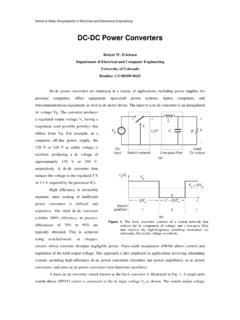
3 Diagrams of the two buck converter switching states in continuous conduction mode are shown in Figure 1. A simplified switch node voltage (VSW) and inductor current waveform are shown in Figure 2. While other converter topologies, like the boost converter , buck -boost converter , series capacitor buck converter [1][2] and many others may also be used, this discussion focuses on the buck converter for 2 buck converter switching waveforms depicting the switch node voltage and the inductor 5 Figure 1 buck converter switching states with (a) high-side switch on and (b) low-side switch LOUT VOUT VOUT COUT COUT (a) (b)Switching PeriodQ1(ON)Q2(ON)VSW(V)VIN00IL(A)tt IL = VL t/L5-2 Topic 5II.
4 MInIMuM on-tIMe VIolAtIonWhen designing a buck converter , selecting the switching frequency (fSW) is typically one of the first design choices to be made. The fSW is selected based on the input voltage, output voltage and other specifications of the buck converter IC. Figure 3 shows an example VSW and VOUT ripple for a buck converter in normal operation. The converter is operating with the following conditions: VIN = 11 V, VOUT = V, IOUT = 0 A, fSW = MHz and forced continuous conduction mode (FCCM). In Figure 4, VIN is increased to 12 V and the VOUT ripple increases. Why does the VOUT ripple increase?Figure 3 11 V input switching node and output voltage ripple 4 12 V input switching node and output voltage ripple increased output voltage ripple in this waveform is a result of a violation of the minimum on-time of the buck converter IC.
5 Equation (1) is a simple equation to estimate the on-time of the converter . This equation ignores losses in the converter for simplicity. When there is no load, the losses are low so this equation is an accurate estimation for no load. When the output is loaded and there are more losses in the converter , the on-time increases. The calculated on-time required for VIN = 12 V, VOUT = V and fSW = MHz is 83 ns. The estimated on-time is below the typical 90 ns minimum on-time for the converter [3]. (1)The converter used in this example is a fixed frequency converter . When the on-time required is less than the minimum on-time, the converter skips switching pulses to keep VOUT regulated.
6 The converter outputs a series of 90 ns minimum on-time pulses that charge VOUT above the target regulated voltage. The control loop responds to the overcharged VOUT with a skipped pulse to regulate VOUT to the correct DC voltage. Other Converters may respond differently when the minimum on-time is violated. For example, the fSW may begin to decrease or VOUT may become regulated to a higher avoid potential problems related to the minimum on-time, the switching frequency should be selected considering the maximum input voltage and maximum minimum on-time listed in the datasheet. The maximum minimum on-time should be used because the minimum on-time typically varies with temperature, with output current and between parts.
7 Figure 5 shows an example of how the minimum on-time can vary with temperature and load [3]. Typically, a number for the maximum minimum on-time is given in the electrical specifications of the datasheet. Using this number is the most conservative the maximum minimum on-time is found, Equation (2) can be used to calculate the maximum fSW. The part used in this example is specified for a maximum minimum on-time of 130 ns [3]. Using this with the VIN and VOUT in this example, the fSW should be set below 769 kHz to always avoid (5 V/div) VOUT (20 mV/div) 2 s/div SW (5 V/div) VOUT (20 mV/div) 2 s/div tON=1fSW VOUTVINtON=83 ns5-3 Topic 5 Figure 5 Example variation in minimum on-time with temperature and load.
8 (2)Violation of the minimum on-time is not the only possible cause of increased output voltage ripple. For example, an unstable control loop or poor PCB layout are other possible causes. Some of these different causes will be discussed in later sections of this derAtIngAnother important consideration when selecting a part for an application is thermal performance. It is best to keep the operating temperature of the part as low as possible. In extreme cases, high operating temperature may cause a part to operate above its rated junction temperature and reach thermal shutdown. It can also reduce the lifetime of an IC as higher temperature accelerates 6 shows the thermal image of two different Converters both operating with the following conditions: VIN = 12 V, VOUT = V, IOUT = 8 A, and fSW = 700 kHz.
9 Part A has a case temperature TC = C and Part B has TC = C. In addition to a higher TC, the thermal image for Part B shows higher PCB temperature and a larger thermal footprint. Part B would have little thermal margin in an application requiring operation up to an ambient temperature of 85 C. Which of these two parts are rated for 8 A?It turns out, both Part A and Part B are rated for 8 A! Table 1 gives a full comparison of the specifications for these two parts. Part A and Part B have similar specifications except for one important parameter; Part B is designed with higher RDS(ON) MOSFETs than Part A resulting in more power dissipation in Part B. Higher RDS(ON) MOSFETs can be advantageous in applications where optimizing cost is more important than optimizing efficiency.
10 SpecPart A (TPS54824)Part B (TPS54821)VIN 17 17 VCurrent8 A8 x x mmRDS(ON)14/6 m 26/19 m Modeled WSimulated die temp64 C81 CPrice$$$Table 1 Specification comparison between Part A and Part 1tON( MIN ) VOUTVIN( MAX )Figure 6 Thermal image for two parts operating in the same load conditions. TPS54824 TPS54821 Part A Inductor Part B Inductor 5-4 Topic 5 Why is Part B rated for 8 A? Part B may be a good choice for applications which do not require operation in higher ambient temperatures. There are also two possible application specific details which allow Part B to better support an 8 A application. First, to reduce the operating temperature of Part B, the power loss could be reduced by designing for a lower fSW.