Transcription of LM2576 - 3.0 A, 15 V, Step-Down Switching Regulator
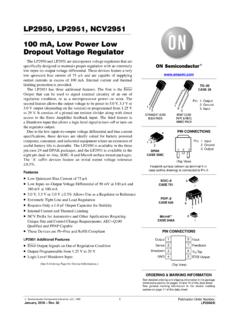
1 Semiconductor Components Industries, LLC, 2006 January, 2006 Rev. 81 Publication Order Number: LM2576 A, 15 V, Step DownSwitching RegulatorThe LM2576 series of regulators are monolithic integrated circuitsideally suited for easy and convenient design of a step downswitching Regulator (buck converter). All circuits of this series arecapable of driving a A load with excellent line and load devices are available in fixed output voltages of V, V,12 V, 15 V, and an adjustable output regulators were designed to minimize the number of externalcomponents to simplify the power supply design.
2 Standard series ofinductors optimized for use with the LM2576 are offered by severaldifferent inductor the LM2576 converter is a switch mode power supply, itsefficiency is significantly higher in comparison with popularthree terminal linear regulators, especially with higher input many cases, the power dissipated is so low that no heatsink isrequired or its size could be reduced standard series of inductors optimized for use with the LM2576are available from several different manufacturers.
3 This featuregreatly simplifies the design of switch mode power LM2576 features include a guaranteed 4% tolerance on outputvoltage within specified input voltages and output load conditions, and 10% on the oscillator frequency ( 2% over 0 C to 125 C). Externalshutdown is included, featuring 80 mA (typical) standby current. Theoutput switch includes cycle by cycle current limiting, as well asthermal shutdown for full protection under fault V, V, 12 V, 15 V, and Adjustable Output Versions Adjustable Version Output Voltage Range, to 37 V 4%Maximum Over Line and Load Conditions Guaranteed A Output Current Wide Input Voltage Range Requires Only 4 External Components 52 kHz Fixed Frequency Internal Oscillator TTL Shutdown Capability.
4 Low Power Standby Mode High Efficiency Uses Readily Available Standard inductors Thermal Shutdown and Current Limit Protection Moisture Sensitivity Level (MSL) Equals 1 Pb Free Packages are AvailableApplications Simple High Efficiency Step Down (Buck) Regulator Efficient Pre Regulator for Linear Regulators On Card Switching Regulators Positive to Negative Converter (Buck Boost) Negative Step Up Converters Power Supply for Battery ChargersSee detailed ordering and shipping information in the packagedimensions section on page 24 of this data INFORMATION15TO 220TV SUFFIXCASE 314B15 Heatsink surface connected to Pin 3TO 220T SUFFIXCASE 314 DPin1.
5 Vin2. Output3. Ground4. Feedback5. ON/OFFD2 PAKD2T SUFFIXCASE 936 AHeatsink surface (shown as terminal 6 incase outline drawing) is connected to Pin 315 general marking information in the device markingsection on page 25 of this data MARKING INFORMATIONLM2576 1. Block Diagram and Typical V 40 VUnregulated DC InputL1100 mHGND+Vin1 Cin100 mF3ON/OFF5 Output2 Feedback4D11N5822 Cout1000 mFTypical Application (Fixed Output Voltage Versions)Representative Block Diagram and Typical ApplicationUnregulatedDC Input+ kOutput2 GND3ON/OFF5 ResetLatchThermalShutdown52 VBand GapReferenceFreqShift18 kHzComparatorFixed GainError V InternalRegulatorRegulatedOutputVoutLoad OutputVoltage V12 V15 VR2(W)
6 KFor adjustable versionR1 = open, R2 = 0 V Regulated Output A LoadThis device contains 162 active RATINGSR atingSymbolValueUnitMaximum Supply VoltageVin45 VON/OFF Pin Input Voltage V V +VinVOutput Voltage to Ground (Steady State) DissipationCase 314B and 314D (TO 220, 5 Lead)PDInternally LimitedWThermal Resistance, Junction to AmbientRqJA65 C/WThermal Resistance, Junction to C/WCase 936A (D2 PAK)PDInternally LimitedWThermal Resistance, Junction to AmbientRqJA70 C/WThermal Resistance, Junction to C/WStorage Temperature RangeTstg 65 to +150 CMinimum ESD Rating (Human Body Model: C = 100 pF, R = kW) Temperature (Soldering, 10 seconds) 260 CMaximum Junction TemperatureTJ150 CMaximum ratings are those values beyond which device damage can occur.
7 Maximum ratings applied to the device are individual stress limitvalues (not normal operating conditions) and are not valid simultaneously. If these limits are exceeded, device functional operation is not implied,damage may occur and reliability may be RATINGS (Operating Ratings indicate conditions for which the device is intended to be functional, but do not guaranteespecific performance limits. For guaranteed specifications and test conditions, see the Electrical Characteristics.)RatingSymbolValueUnitOp erating Junction Temperature RangeTJ 40 to +125 CSupply VoltageVin40 VSYSTEM PARAMETERS (Note 1 Test Circuit Figure 15)ELECTRICAL CHARACTERISTICS (Unless otherwise specified, Vin = 12 V for the V, V, and Adjustable version, Vin = 25 Vfor the 12 V version, and Vin = 30 V for the 15 V version.)
8 ILoad = 500 mA. For typical values TJ = 25 C, for min/max values TJ is theoperating junction temperature range that applies Note 2, unless otherwise noted.)CharacteristicsSymbolMinTypMaxUni tLM2576 (Note 1 Test Circuit Figure 15)Output Voltage (Vin = 12 V, ILoad = A, TJ = 25 C) Voltage ( V Vin 40 V, A ILoad A)VoutVTJ = 25 = 40 to +125 (Vin = 12 V, ILoad = A) 75 % LM2576 5 (Note 1 Test Circuit Figure 15)Output Voltage (Vin = 12 V, ILoad = A, TJ = 25 C) Voltage ( V Vin 40 V, A ILoad A)VoutVTJ = 25 = 40 to +125 (Vin = 12 V, ILoad = A) 77 % LM2576 12 (Note 1 Test Circuit Figure 15)
9 Output Voltage (Vin = 25 V, ILoad = A, TJ = 25 C) Voltage (15 V Vin 40 V, A ILoad A)VoutVTJ = 25 = 40 to +125 (Vin = 15 V, ILoad = A) 88 % LM2576 15 (Note 1 Test Circuit Figure 15)Output Voltage (Vin = 30 V, ILoad = A, TJ = 25 C) Voltage (18 V Vin 40 V, A ILoad A)VoutVTJ = 25 = 40 to +125 (Vin = 18 V, ILoad = A) 88 % LM2576 ADJUSTABLE VERSION (Note 1 Test Circuit Figure 15)Feedback Voltage (Vin = 12 V, ILoad = A, Vout = V, TJ = 25 C) Voltage ( V Vin 40 V, A ILoad A, Vout = V)VoutVTJ = 25 = 40 to +125 (Vin = 12 V, ILoad = A, Vout = V) 77 %1.
10 External components such as the catch diode, inductor, input and output capacitors can affect Switching Regulator system the LM2576 is used as shown in the Figure 15 test circuit, system performance will be as shown in system parameters Tested junction temperature range for the LM2576 : Tlow = 40 C Thigh = +125 CLM2576 PARAMETERSELECTRICAL CHARACTERISTICS (Unless otherwise specified, Vin = 12 V for the V, V, and Adjustable version, Vin = 25 Vfor the 12 V version, and Vin = 30 V for the 15 V version.)
