Transcription of DRV5055 Ratiometric Linear Hall Effect Sensor …
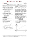
1 BsouthnorthOUT0 mT0 VVCCVL (MIN)VL (MAX)VCC / 2 OUTDRV5055 VCCC ontrollerVCCGNDADCC opyright 201 7, texas Instrumen ts Incorpor ate dProductFolderOrderNowTechnicalDocuments Tools &SoftwareSupport &CommunityAn IMPORTANTNOTICEat the end of this datasheetaddressesavailability,warranty, changes,use in safety-criticalapplications,intellectual propertymattersand JANUARY2018 DRV5055 RatiometricLinearHall EffectSensor11 Features1 RatiometricLinearHall EffectMagneticSensor 5-V PowerSupplies AnalogOutputWithVCC/ 2 QuiescentOffset MagneticSensitivityOptions(At VCC= 5 V): A1: 100 mV/mT, 21-mTRange A2: 50 mV/mT, 42-mTRange A3: 25 mV/mT, 85-mTRange A4: , 169-mTRange Fast20-kHzSensingBandwidth Low-NoiseOutputWith 1-mADrive CompensationFor MagnetTemperatureDrift StandardIndustryPackages.
2 Surface-MountSOT-23 Through-HoleTO-922 Applications PrecisePositionSensing IndustrialAutomationand Robotics HomeAppliances Gamepads,Pedals,Keyboards,Triggers HeightLeveling,Tilt and WeightMeasurement FluidFlowRateMeasurement MedicalDevices AbsoluteAngleEncoding CurrentSensing3 DescriptionTheDRV5055deviceis a linearHalleffectsensorthat respondsproportionallyto magneticflux devicecan be usedfor accuratepositionsensingin a widerangeof magneticfieldis present,theanalogoutputdriveshalf of VCC. The outputchangeslinearlywiththe appliedmagneticflux density,andfour sensitivityoptionsenablemaximaloutputvol tageswingbasedon the perpendicularto the top of the packageis sensed,andthe deviceusesa ratiometricarchitecturethat caneliminateerrorfromVCCtolerancewhenthe externalanalog-to-digitalconverter(ADC)u sesthe sameVCCfor its ,the devicefeaturesmagnettemperaturecompensat ionto counteracthowmagnetsdrift for linearperformanceacrossa wide 40 C to 125 C (1)PARTNUMBERPACKAGEBODYSIZE(NOM) DRV5055 SOT-23(3) (3) (1) For all availablepackages,see the orderableaddendumatthe end of the.
3 DRV5055 SubmitDocumentationFeedbackCopyright 2018,TexasInstrumentsIncorporatedTableof Contents1 Pin Configurationand Applicationand 's and Don'ts ..169 Deviceand Mechanical,Packaging,and RevisionHistoryNOTE:Pagenumbersfor previousrevisionsmay differfrompagenumbersin the * JANUARY2018 ProductFolderLinks: DRV5055 SubmitDocumentationFeedbackCopyright 2018,TexasInstrumentsIncorporated5 Pin Configurationand FunctionsDBZP ackage3-PinSOT-23 Top ViewLPGP ackage3-PinTO-92 Top ViewPin FunctionsPINI/ODESCRIPTIONNAMESOT-23TO-9 2 VCC11 recommendsconnectingthis pin to a ceramiccapacitorto groundwith a valueof at Groundreference(1)Stressesbeyondthoselis tedunderAbsoluteMaximumRatingsmay causepermanentdamageto the stressratingsonly,whichdo not implyfunctionaloperationof the deviceat theseor any otherconditionsbeyondthoseindicatedunder RecommendedOperatingConditions.
4 Exposureto absolute-maximum-ratedconditionsfor extendedperiodsmay (unlessotherwisenoted)(1)MINMAXUNITP owersupplyvoltageVCC + density,BMAXU nlimitedTOperatingjunctiontemperature,TJ 40150 CStoragetemperature,Tstg 65150 C4 DRV5055 SBAS640 : DRV5055 SubmitDocumentationFeedbackCopyright 2018,TexasInstrumentsIncorporated(1)JEDE C documentJEP155statesthat 500-VHBM allowssafe manufacturingwith a standardESDcontrolprocess.(2)JEDEC documentJEP157statesthat 250-VCDM allowssafe manufacturingwith a (ESD)ElectrostaticdischargeHuman-bodymod el(HBM),per ANSI/ESDA/JEDECJS-001(1) 2500 VCharged-devicemodel(CDM),per JEDEC specificationJESD22-C101(2) 750(1)Thereare two moreinformationsee theOperatingVCCR angessection.
5 (2)Powerdissipationand thermallimitsmustbe (unlessotherwisenoted)MINMAXUNITVCCP owersupplyvoltage(1) 11mATAO peratingambienttemperature(2) 40125 C(1)For moreinformationabouttraditionaland new thermalmetrics,see (1) DRV5055 UNITSOT-23(DBZ)TO-92(LPG)3 PINS3 PINSR JAJunction-to-ambientthermalresistance17 0121 C/WR JC(top)Junction-to-case(top)thermalresis tance6667 C/WR JBJunction-to-boardthermalresistance4997 C/WYJBJ unction-to-boardcharacterizationparamete r4897 C/W(1)B is the appliedmagneticflux density.(2)VNdescribesvoltagenoiseon the the full devicebandwidthis not needed,noisecan be reducedwith an RC VCC= 3 V to and V to V, overoperatingfree-airtemperaturerange(un lessotherwisenoted)PARAMETERTESTCONDITIO NS(1)MINTYPMAXUNITICCO peratingsupplycurrent610mAtONPower-ontim e (seeFigure11)B = 0 mT, no load on OUT175330 sfBWSensingbandwidth20kHztdPropagationde laytimeFromchangein B to changein OUT10 sBNDI nput-referredRMSnoisedensityVCC= 5 V130nT/ HzVCC= V215 BNInput-referrednoiseBND 20 kHzVCC= 5 (2)BN JANUARY2018 ProductFolderLinks.
6 DRV5055 SubmitDocumentationFeedbackCopyright 2018,TexasInstrumentsIncorporated(1)B is the appliedmagneticflux density.(2)See theRatiometricArchitecturesection.(3)BLd escribesthe minimumlinearsensingrangeat 25 C takinginto accountthe maximumVQand Sensitivitytolerances.(4)See theSensitivityLinearitysection.(5)STCdes cribesthe rate the deviceincreasesSensitivitywith moreinformation,see VCC= 3 V to and V to V, overoperatingfree-airtemperaturerange(un lessotherwisenoted)PARAMETERTESTCONDITIO NS(1)MINTYPMAXUNITVQQ uiescentvoltageB = 0 mT, TA= 25 CVCC= 5 TQuiescentvoltagetemperaturedriftB = 0 mT,TA= -40 C to 125 C versus25 C 1% VCCVVQREQ uiescentvoltageratiometryerror(2) LQuiescentvoltagelifetimedriftHigh-tempe ratureoperatingstressfor1000hours< 5 V,TA= 25 CDRV5055A195100105 V,TA= 25 (3)(4)
7 VCC= 5 V,TA= 25 CDRV5055A1 21mTDRV5055A2 42 DRV5055A3 85 DRV5055A4 169 VCC= V,TA= 25 CDRV5055A1 22 DRV5055A2 44 DRV5055A3 88 DRV5055A4 176 VLLinearrangeof outputvoltage(4) magnets(5) CSLES ensitivitylinearityerror(4)VOUTis withinVL 1%SSES ensitivitysymmetryerror(4)VOUTis withinVL 1%SRES ensitivityratiometryerror(2)TA= 25 C,with respectto VCC= V or 5 V LSensitivitylifetimedriftHigh-temperatur eoperatingstressfor1000hours< Voltage (V)Sensitivity (mV/mT) Voltage (V)Sensitivity (mV/mT) (qC)Sensitivity (mV/mT)-40-20020406080100120140020406080 D004 DRV5055A1 DRV5055A2 DRV5055A3 DRV5055A4 Temperature (qC)Sensitivity (mV/mT)-40-20020406080100120140020406080 100120D005 DRV5055A1 DRV5055A2 DRV5055A3 DRV5055A4 Temperature (qC)Quiescent Voltage (V) = VVCC = 5 VSupply Voltage (V)Quiescent Voltage (V) : DRV5055 SubmitDocumentationFeedbackCopyright 2018, TA= 25 C (unlessotherwisenoted)Figure1.
8 QuiescentVoltagevs TemperatureFigure2. QuiescentVoltagevs SupplyVoltageFigure3. Sensitivityvs Temperature,VCC= VFigure4. Sensitivityvs Temperature,VCC= 5 VFigure5. Sensitivityvs SupplyVoltage,VCC= V 10%Figure6. Sensitivityvs SupplyVoltage,VCC= 5 V 10%Temperature (qC)Operating Supply Current (mA) = VVCC = 5 JANUARY2018 ProductFolderLinks: DRV5055 SubmitDocumentationFeedbackCopyright 2018,TexasInstrumentsIncorporatedTypical Characteristics(continued)for TA= 25 C (unlessotherwisenoted)Figure7. OperatingSupplyCurrentvs F(minim um) VCCO utput DriverOUTGNDVCC Optional filterElement BiasOffset CancellationTemperature CompensationPrecision AmplifierBandgap ReferenceTrim RegistersCopyright 201 7, texas Instrumen ts Incorpor ate d8 DRV5055 SBAS640.
9 DRV5055 SubmitDocumentationFeedbackCopyright 2018,TexasInstrumentsIncorporated7 a 3-pinlinearHalleffectsensorwithfullyinte gratedsignalconditioning,temperaturecomp ensationcircuits,mechanicalstresscancell ation,and 5-V( 10%)powersupplies,measuresmagneticflux density,and outputsa proportionalanalogvoltagethat isreferencedto shownin Figure8, the DRV5055is sensitiveto the magneticfield componentthat is perpendicularto the topof the Directionof SensitivityVOUT = VQ + B Sensitivity(25 C) (1 + STC (TA 25 C))() JANUARY2018 ProductFolderLinks: DRV5055 SubmitDocumentationFeedbackCopyright 2018,TexasInstrumentsIncorporatedFeature Description(continued)Magneticflux that travelsfromthe bottomto the top of the packageis consideredpositivein this southmagneticpoleis nearthe top (marked-side)of the thattravelsfromthe top to the bottomof the packageresultsin The FluxDirectionfor DRV5055is powered,the DRV5055outputsan analogvoltageaccordingto Equation1.
10 Where VQis typicallyhalf of VCC B is the appliedmagneticflux density Sensitivity(25 C)dependson the deviceoptionand VCC STCis C TAis the ambienttemperature VOUTis withinthe VLrange(1)As an example,considerthe DRV5055A3withVCC= V, a temperatureof 50 C, and 67 mT ,VOUT= 1650mV + 67 mT (15 mV/mT (1 + C (50 C 25 C))) = deviceproducesa linearresponsewhenthe outputvoltageis withinthe ,sensitivityis reducedand graphsthe (VCC) / VQ( )1 VCC / =for VCC = 3 V to VVQ(VCC) / VQ(5V)1 VCC / 5 VVQRE =for VCC = V to V,S(VCC) / S( )1 VCC / =for VCC = 3 V to VS(VCC) / S(5V)1 VCC / 5 VSRE =for VCC = V to V,VL(MAX) VQ(MAX)S(MAX)BL(MIN) =BsouthnorthOUT0 mT0 VVCCVL (MIN)VL (MAX)VCC / 210 DRV5055 SBAS640 : DRV5055 SubmitDocumentationFeedbackCopyright 2018,TexasInstrumentsIncorporatedFeature Description(continued)Figure10.