Transcription of EPC2302 – Enhancement Mode Power Transistor
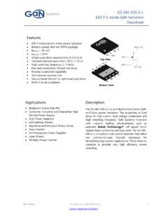
1 EGaN FET DATASHEET EPC2302 . EPC2302 Enhancement Mode Power Transistor D. VDS , 100 V G. RDS(on) , m max EFFICIENT Power CONVERSION. S HAL. General Description The EPC2302 is a m max RDS(on), 100 V eGaN Power Transistor in a low inductance 3 x 5 mm QFN. package with exposed top for excellent thermal management. It is tailored to high frequency DC-DC. 23 PC. X W. X YY 2. X W. X 0. E. applications to/from 40 V 60 V and 48 V BLDC motor drives. X. The thermal resistance to case top is ~ C/W, resulting in excellent thermal behavior and easy cooling. The device features an enhanced PQFN Thermal-Max package. The exposed top enhances EPC2302 . top-side thermal management and the side-wettable flanks guarantee that the complete side-pad Package size: 3 x 5 mm surface is wetted with solder during the reflow soldering process, which protects the copper and allows soldering to occur on this external flank area for easy optical inspection.
2 Features 100 V. Compared to a Si MOSFET, the footprint of 15 mm2 is less than half of the size of the best-in-class Si m typical, m max RDS(on). MOSFET with similar Rds(on) and voltage rating, QG and QGD are significantly smaller and QRR is 0. 3 x 5 mm QFN package This results in lower switching losses and lower gate driver losses. Moreover, EPC2302 is very fast Exposed top for top-side thermal management and can operate with deadtime less than 10 ns for higher efficiency and QRR = 0 is a big advantage Moisture rating MSL2. for reliability and EMI. In summary, EPC2302 allows the highest Power density due to enhanced Enhanced Thermal-Max package efficiency, smaller size, and higher switching frequency for smaller inductor and fewer capacitors.
3 The EPC2302 enables designers to improve efficiency and save space. The excellent thermal behavior Applications enables easier and lower cost cooling. The ultra-low capacitance and zero reverse recovery of the AC-DC chargers, SMPS, adaptors, Power supplies eGaN FET enables efficient operation in many topologies. Performance is further enhanced due to High Frequency DC-DC Conversion up to 80 V. the small, low inductance footprint. input (Buck, Boost, Buck-Boost and LLC). 24 V 60 V Motor Drives Application notes: High Power Density DC-DC modules from Easy-to-use and reliable gate, Gate Drive ON = 5 V typical, OFF = 0 V (negative voltage not needed) 40 V 60 V to 5 V 12 V.
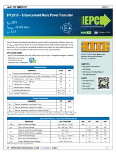
4 Top of FET is electrically connected to source Synchronous Rectification Questions: Ask a GaN Expert Solar MPPT. Benefits Maximum Ratings Ultra High Efficiency PARAMETER VALUE UNIT No Reverse Recovery VDS Drain-to-Source Voltage (Continuous) 100 Ultra Low QG. V. Drain-to-Source Voltage (up to 10,000 5 ms pulses at 150 C) 120 Small Footprint Continuous (TA = 25 C) 101 Excellent Thermal ID A. Pulsed (25 C, TPULSE = 300 s) 408. Gate-to-Source Voltage 6. VGS V. Gate-to-Source Voltage -4. TJ Operating Temperature 40 to 150. C. TSTG Storage Temperature 40 to 150. EPC Power CONVERSION TECHNOLOGY LEADER | | 2022 | | 1. eGaN FET DATASHEET EPC2302 . Thermal Characteristics PARAMETER TYP UNIT.
5 R JC Thermal Resistance, Junction-to-Case (Case TOP) R JB Thermal Resistance, Junction-to-Board (Case BOTTOM) C/W. R JA_JEDEC Thermal Resistance, Junction-to-Ambient (using JEDEC 51-2 PCB) 45. R JA_EVB Thermal Resistance, Junction-to-Ambient (using EPC90142 EVB) 21. Static Characteristics (TJ = 25 C unless otherwise stated). PARAMETER TEST CONDITIONS MIN TYP MAX UNIT. BVDSS Drain-to-Source Voltage VGS = 0 V, ID = mA 100 V. IDSS Drain-Source Leakage VDS = 80 V, VGS = 0 V 1 100 A. Gate-to-Source Forward Leakage VGS = 5 V 4. IGSS Gate-to-Source Forward Leakage# VGS = 5 V, TJ = 125 C 9 mA. Gate-to-Source Reverse Leakage VGS = -4 V VGS(TH) Gate Threshold Voltage VDS = VGS, ID = 14 mA V.
6 RDS(on) Drain-Source On Resistance VGS = 5 V, ID = 50 A m . VSD Source-to-Drain Forward Voltage IS = A, VGS = 0 V V. # Defined by design. Not subject to production test. Dynamic Characteristics# (TJ = 25 C unless otherwise stated). PARAMETER TEST CONDITIONS MIN TYP MAX UNIT. CISS Input Capacitance 3200 4800. CRSS Reverse Transfer Capacitance VDS = 50 V, VGS = 0 V 7. COSS Output Capacitance 1000 1200 pF. COSS(ER) Effective Output Capacitance, Energy Related (Note 1) 1300. VDS = 0 to 50 V, VGS = 0 V. COSS(TR) Effective Output Capacitance, Time Related (Note 2) 1700. RG Gate Resistance . QG Total Gate Charge VDS = 50 V, VGS = 5 V, ID = 50 A 23 29.
7 QGS Gate-to-Source Charge QGD Gate-to-Drain Charge VDS = 50 V, ID = 50 A nC. QG(TH) Gate Charge at Threshold QOSS Output Charge VDS = 50 V, VGS = 0 V 85 94. QRR Source-Drain Recovery Charge 0. # Defined by design. Not subject to production test. Note 1: COSS(ER) is a fixed capacitance that gives the same stored energy as COSS while VDS is rising from 0 to 50% BVDSS. Note 2: COSS(TR) is a fixed capacitance that gives the same charging time as COSS while VDS is rising from 0 to 50% BVDSS. EPC Power CONVERSION TECHNOLOGY LEADER | | 2022 | | 2. eGaN FET DATASHEET EPC2302 . Figure 1: Typical Output Characteristics at 25 C Figure 2: Typical Transfer Characteristics 400 400.
8 350 350. 25 C. 300 300 125 C. VGS = 5 V. ID Drain Current (A). ID Drain Current (A). VGS = 4 V VDS = 3 V. 250 250. VGS = 3 V. VGS = 2 V. 200 200. 150 150. 100 100. 50 50. 0 0. 0 VDS Drain-to-Source Voltage (V) VGS Gate-to-Source Voltage (V). Figure 3: Typical RDS(on) vs. VGS for Various Drain Currents Figure 4: Typical RDS(on) vs. VGS for Various Temperatures 6 6. RDS(on) Drain-to-Source Resistance (m ). 5 ID = 25 A RDS(on) Drain-to-Source Resistance (m ) 5 25 C. ID = 50 A. 125 C. ID = 75 A. 4 ID = 100 A 4 ID = 50 A. 3 3. 2 2. 1 1. 0 0. VGS Gate-to-Source Voltage (V) VGS Gate-to-Source Voltage (V). Figure 5a: Typical Capacitance (Linear Scale) Figure 5b: Typical Capacitance (Log Scale).
9 4000 10000. COSS = CGD + CSD. CISS = CGD + CGS. 3000 CRSS = CGD 1000. Capacitance (pF). Capacitance (pF). COSS = CGD + CSD. CISS = CGD + CGS. 2000 100 CRSS = CGD. 1000 10. 0 1. 0 25 50 75 100 0 25 50 75 100. VDS Drain-to-Source Voltage (V) VDS Drain-to-Source Voltage (V). EPC Power CONVERSION TECHNOLOGY LEADER | | 2022 | | 3. eGaN FET DATASHEET EPC2302 . Figure 6: Typical Output Charge and COSS Stored Energy Figure 7: Typical Gate Charge 5. 120 ID = 50 A. 4. EOSS COSS Stored Energy ( J). VDS = 50 V. VGS Gate-to-Source Voltage (V). QOSS Output charge (nC). 90 3. 60 2. 30 1. 0. 0. 0 20 40 60 80 100 0 5 10 15 20 25. VDS Drain-to-Source Voltage (V) QG Gate Charge (nC).
10 Figure 8: Typical Reverse Drain-Source Characteristics Figure 9: Typical Normalized On-State Resistance vs. Temp. 400 Normalized On-State Resistance RDS(on). 350 25 C. 125 C. ISD Source-to-Drain Current (A). 300 ID = 50 A. VGS = 0 V. VGS = 5 V. 250. 200 150. 100 50. 0 0 0 25 50 75 100 125 150. VSD Source-to-Drain Voltage (V) TJ Junction Temperature ( C). Figure 10: Typical Normalized Threshold Voltage vs. Temp. Figure 11: Safe Operating Area 1000. Limited by RDS(on). Normalized Threshold Voltage ID = 14 mA 100. I D Drain Current (A). 10. Pulse Width 1 ms 100 ms 1. 10 ms100 s 1 ms 10 s 100 s 0 25 50 75 100 125 150 1 10 100 1000. TJ Junction Temperature ( C) VDS Drain-Source Voltage (V).