Transcription of High-Speed, 4-A, 600-V High-Side Low-Side Gate Driver (Rev. …
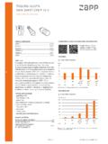
1 7 VDD1 HI2 LI3 VSS4 EN/NC5 COM131211 HBHOHSRLORHOUCC277146 LOLoad10 k:10 k:CBOOTQ1Q2 RBOOTCVDDCHICLIRLIRHIC ontrollerVSSPWM2 PWM1 ENRBIASBiasDBOOTUp to 600 V507090110130150170190210230250 40 20 020406080100120 Propagation Delay (ns) Temperature ( C) CompetitorTIC037 ProductFolderOrderNowTechnicalDocumentsT ools &SoftwareSupport &CommunityAn IMPORTANTNOTICEat the end of this datasheetaddressesavailability,warranty, changes,use in safety-criticalapplications,intellectual propertymattersand AUGUST2015 REVISEDMARCH2017 UCC27714 high -Speed, 600-V high -SideLow-SideGate Driverwith 4-A Peak Output11 Features1 High-Side ,Low-SideConfiguration,withInde pendentInputs FullyOperationalup to 600 V (HS Pin)
2 FloatingChannelDesignedfor BootstrapOperation PeakOutputCurrentCapabilityof 4-A Sink4-ASourceat VDD= 15 V Best-In-ClassPropagationDelay(125-nsMaxi mum) Best-In-ClassDelayMatching(20-nsMaximum) TTL and CMOSC ompatibleInputLogic VDDBiasSupplyRangeof 10 V to 20 V BiasUVLOP rotectionfor BothChannels Rail-to-RailDrive RobustOperationUnderNegativeVoltageTrans ients Highdv/dtImmunity(HS Pin) SeparatedGroundsfor Logic(VSS)and Driver (COM)with Capabilityto SustainVoltageDifference OptionalEnableFunction(Pin 4) OutputsHeldin LOWwhenInputsFloating Inputsand EnablePin VoltageLevelsNotRestrictedby VDDPin BiasSupplyVoltage Highand Low VoltagePinsSeparatedforMaximumCreepagean d Clearance NegativeVoltageHandlingCapabilityon InputandEnablePins(1)
3 For all availablepackages,see the orderableaddendumatthe end of the Applications Half-Bridgeand Full-BridgeConvertersin OfflineAC and DC PowerSupplies high -DensitySwitchingPowerSuppliesforSer ver,Telecom,IT and IndustrialInfrastructure SolarInverters,MotorDriveand UPS3 DescriptionUCC27714is a 600-Vhigh- side ,low-sidegatedriverwith4-A sourceand4-Asinkcurrentcapability,target edto drivepowerMOSFETsor one ground-referencedchannel(LO)and one floatingchannel(HO)whichis designedfor maintainoperationallogicatnegativevoltag esof up to 8 VDCon HS pin (at VDD= 12 V).The deviceacceptsa widerangebiassupplyinputfrom10 V to 20 V and offersUVLO protectionforboththe VCCand HB bias SOIC-14packageand ratedto operatefrom 40 C to 125 (1)PARTNUMBERPACKAGEBODYSIZE(NOM)UCC2771 4 SOIC(14) AUGUST2015 :UCC27714 SubmitDocumentationFeedbackCopyright 2015 2017,TexasInstrumentsIncorporatedTableof Contents1 Pin Configurationand Applicationand Deviceand Mechanical,Packaging,and RevisionHistoryChangesfromRevisionA (August2015)to RevisionBPage ChangedMAXS upplyvoltagefrom18 V to 17 V.
4 5 ChangedMAXD riverbootstrapvoltagefrom18 V to 17 V..5 ChangedMAXB ootstrappin voltagefrom18 V to 17 ChangedMAXI nputvoltagewith respectto VSSfrom18 V to 17 V..5 Added40 ns NOMto Added40 ns NOMto Deleted18-Vreferencefromall ChangedNegativeVoltageChartTimevs AddedIncreaseRHOand RLO, ReduceHS dV/dtimageand AddedLO and HO Overshootand (August,2015)to RevisionAPage ChangedmarketingstatusfromProductpreview to ` AUGUST2015 REVISEDMARCH2017 ProductFolderLinks:UCC27714 SubmitDocumentationFeedbackCopyright 2015 2017,TexasInstrumentsIncorporated5 Pin Configurationand FunctionsD Package14-PinSOICTop ViewPin Returnfor high -sideand pin biasedLOW,disablesbothHO andLO regardlessof HI and LI state,This pin biasedhigh or floatingenablesbothHO and pin to HS with a suitablecapacitorto sustainboot-strapcircuitoperationin the desiredapplication,typically10 HI is unbiasedor floating,HO is held Returnfor LI is unbiasedor floating,LO is held , 9, 10.
5 14 No the inputlogicside of the deviceand also pin to VSSwith typical1- F SMDcapacitor(typicallyCVDD needsto be10 CBOOT). If shuntresistorusedbetweenCOMand VSS,thenalso bypassthis pin toCOMwith 1- F AUGUST2015 :UCC27714 SubmitDocumentationFeedbackCopyright 2015 2017,TexasInstrumentsIncorporated(1)Stre ssesbeyondthoselistedunderAbsoluteMaximu mRatingsmay causepermanentdamageto the stressratingsonly,whichdo not implyfunctionaloperationof the deviceat theseor any otherconditionsbeyondthoseindicatedunder RecommendedOperatingConditions. Exposureto absolute-maximum-ratedconditionsfor extendedperiodsmay affectdevicereliability.
6 (2)See PackagingSectionof the datasheetfor thermallimitationsand considerationsof packages.(3)The maximumvoltageon the Inputpins is not restrictedby the voltageon the VDDpin.(4)Valuesare verifiedby characterizationon (1) (2)Overoperatingfree-airtemperaturerange (unlessotherwisenoted),all voltagesare with respectto COM(unlessotherwisenoted),currentsare positiveinto and negativeout of the specifiedterminal.(1)MINMAXUNITVINI nputvoltagerangeHI, LI, EN(3)with respectto VSS 520 VVDD supplyvoltage ,HODCHS + ,less than100 ns(4)HS 2HB + ,LODC + ,less than100 ns(4) 2 VDD+ ,Withrespectto COM 76 VLogicground,VDD-VSS ,HO, LO, IOUT_PULSED(100ns) 4 AIOUTO utputcurrent,HO, LO, 5050V/nsLeadtemperature(soldering,10 second)300 CTJJ unctiontemperaturerange 40150 CTstgStoragetemperaturerange-65150 AUGUST2015 REVISEDMARCH2017 ProductFolderLinks:UCC27714 SubmitDocumentationFeedbackCopyright 2015 2017,TexasInstrumentsIncorporated(1)Thes edevicesare sensitiveto electrostaticdischarge.
7 (ESD)(1)ElectrostaticdischargeHumanbodym odel,HBM 1400 VChargedevicemodel,CDM 500V(1)Logicoperationalfor HS of 8 V to 600 V at HB HS = 12 V(2)At VDD COM= 10 V(3)At VDD COM= 15 voltagesare with respectto COM, 40 C < TJ< 125 C, currentsare positiveinto, negativeout of the specifiedterminalsMINNOMMAXUNITVDDS upplyvoltage1017 VHB-HSDriverbootstrapvoltage1017 VHSS ourceterminalvoltage(1) 8600 VHBB ootstrappin voltageHS + 10HS + 17 VHI, LI, ENInputvoltagewith respectto VSS 417 VVSSL ogicground 6(2)5(3)VTJJ unctiontemperature 40125 C(1)For moreinformationabouttraditionaland new thermalmetrics,see theIC PackageThermalMetricsapplicationreport, (1)UCC27714 UNITD (SOIC)PINSR C/WR JC(top)Junction-to-case(top) C/WR C/W C/W C/WR JC(bot)Junction-to-case(bottom)thermalre sistanceN/A C/W6 UCC27714 SLUSBY6B AUGUST2015.
8 UCC27714 SubmitDocumentationFeedbackCopyright 2015 2017,TexasInstrumentsIncorporated(1)ROHr epresentson-resistanceof only the P-ChannelMOSFET devicein pull-upstructureof OutputStage(2)Ensuredby Design,Not testedin VDD= VHB= 15 V, VSS= VHS= 0, all voltagesare with respectto COM,no load on LO and HO, 40 C < TJ< 125 C,currentare positiveinto and negativeout of the specifiedterminal,overoperatingfree-airt emperaturerange(unlessotherwisenoted)PAR AMETERTESTCONDITIONSMINTYPMAXUNITSUPPLYB LOCKVVDD(on)turn-onthresholdvoltageof (off)turn-offthresholdvoltageof (hys)Hysteresisof (on)turn-onthresholdvoltageof (off)turn-offthresholdvoltageof (hys)Hysteresisof VSSandCOMsupplycurrentHI = LI = 0 V or 5 V, DC on/offstate7501050 AIQCOMQ uiescentVDD-COMsupplycurrentHI = LI = 0 V or 5 V, DC on/offstate175350 AIQVSSQ uiescentVDD-VSSsupplycurrentHI = LI = 0 V or 5 V, DC on/offstate550750 AIQBSQ uiescentHB-HSsupplycurrentHI = 0 V or 5 V, HO in DC on/offstate120300 AIBLB ootstrapSupplyLeakageCurrentHB = HS = 600 V20 AINPUTANDENABLEBLOCKVINH, VENHI nputpin (HI or LI) and enablepin(EN) , VENLI nputpin (HI or LI) and enablepin(EN)low ,VENHYSI nputpin (HI or LI)
9 And enablepin(EN) , LI inputlow bias currentHI, LI = 0 V-505 AIINHHI, LI inputhigh bias currentHI, LI = 5 V365 AIENLEN inputlow bias currentVEN= 0 V-90-50 AIENHEN inputhigh bias currentVEN= 5 V-65-25 ARHIPull-downresistoron HI inputpin400k RLIPull-downresistoron LI inputpin400k RENPull-upresistoron enablepin200k OUTPUTBLOCKVDD-VLOHLO outputhigh voltageLI = 5 V, ILO= 20 mA70120mVVHB-VHOHHO outputhigh voltageHI = 5 V, IHO= 20 mA70120mVVLOLLO outputlow voltageLI = 0 V, ILO= 20 mA1535mVVHOLHO outputlow voltageHI = 0 V, IHO= 20 mA2040mVRLOL,RHOL(1)LO, HO outputpull downresistanceILO= 20 mA, IHO= 20 RLOH,RHOHLO, HO outputpull up resistanceILO= 20 mA, IHO= 20 IGPK-(2)HO.
10 LO outputlow shortcircuitpulsedcurrentHI = L = 0 V, HO = LO = 15 V, PW <10 s4 AIGPK+(2)HO. LO outputhigh shortcircuitpulsedcurrentH I= LI = 5 V, HO = LO = 0 V, PW <10 s4 AHI, LIHO, LOtPDLHtPDHLHI, LILOHOtPDRMtPDFMtRISEtFALL50%50%10%90%90 %10% AUGUST2015 REVISEDMARCH2017 ProductFolderLinks:UCC27714 SubmitDocumentationFeedbackCopyright 2015 2017, ,LI to LO, HI to HO, HS = COM= 0 V orHS = 600 V90125nstPDHLTurn-offpropagationdelay,LI to LO, HI to HO, HS = COM= 0 V orHS = 600 V90125nstPDRMLow-to-highdelaymatching,HS = COM= 0 V20nstPDFMHigh-to-lowdelaymatching,HS = COM= 0 V20nstRISETurn-onrise time,10%to 90%,HO/LOwith 1000-pFload1530nstFALLTurn-offfall time,90%to 10%,HO/LOwith 1000-pFload1530nstONMinimumHI/LION pulsethat changesoutputstate,0-V to 5-V inputsignalon HI and LI pins40100nstOFFM inimumHI/LIOFF pulsethat changesoutputstate.