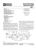
Transcription of MCP6021/1R/2/3/4 - Rail-to-Rail Input/Output, 10 MHz Op ...
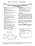
1 MCP6021/1R/2/3/4 . Rail-to-Rail Input/Output, 10 MHz Op Amps Features Description Rail-to-Rail Input/Output The MCP6021, MCP6021R, MCP6022, MCP6023 and Wide Bandwidth: 10 MHz (typical) MCP6024 from Microchip Technology Inc. are rail-to- Low Noise: nV/ Hz at 10 kHz (typical) rail input and output operational amplifiers with high performance. Key specifications include: wide band- Low Offset Voltage: width (10 MHz), low noise ( nV/ Hz), low input offset - Industrial Temperature: 500 V (max.) voltage and low distortion ( THD+N). The - Extended Temperature: 250 V (max.) MCP6023 also offers a Chip Select pin (CS) that gives Mid-Supply VREF: MCP6021 and MCP6023 power savings when the part is not in use.
2 Low Supply Current: 1 mA (typical) The single MCP6021 and MCP6021R are available in Total Harmonic Distortion: SOT-23-5 packages. The single MCP6021, single - (typical, G = 1 V/V) MCP6023 and dual MCP6022 are available in 8-lead PDIP, SOIC and TSSOP packages. The Extended Unity Gain Stable Temperature single MCP6021 is available in 8-lead Power Supply Range: to MSOP. The quad MCP6024 is offered in 14-lead PDIP, Temperature Range: SOIC and TSSOP packages. - Industrial: -40 C to +85 C The MCP6021/1R/2/3/4 family is available in Industrial - Extended: -40 C to +125 C and Extended temperature ranges.
3 It has a power supply range of to Applications Automotive Package Types Multi-Pole Active Filters MCP6021 MCP6022. SOT-23-5 PDIP, SOIC, TSSOP. Audio Processing DAC Buffer VOUT 1 5 VDD VOUTA 1 8 VDD. Test Equipment VSS 2 VINA- 2 7 VOUTB. Medical Instrumentation VIN+ 3 4 VIN- VINA+ 3 6 VINB- VSS 4 5 VINB+. Design Aids MCP6021R. SOT-23-5 MCP6023. SPICE Macro Models PDIP, SOIC, TSSOP. FilterLab Software VOUT 1 5 VSS. MPLAB Mindi Analog Simulator VDD 2 NC 1 8 CS. Microchip Advanced Part Selector (MAPS) VIN+ 3 4 VIN- VIN- 2 7 VDD. Analog Demonstration and Evaluation Boards VIN+ 3 6 VOUT.
4 Application Notes MCP6021 VSS 4 5 VREF. PDIP, SOIC, MSOP, TSSOP MCP6024. Typical Application PDIP, SOIC, TSSOP. pF. NC 1 8 NC. 7 VDD VOUTA 1 14 VOUTD. Photo Detector VIN- 2. 100 k VIN+ 3 6 VOUT VINA- 2 13 VIND- VSS 4 5 V VINA+ 3 12 VIND+. REF. 100 pF VDD 4 11 VSS. MCP6021 VINB+ 5 10 VINC+. VDD/2 VINB- 6 9 VINC- Transimpedance Amplifier VOUTB 7 8 VOUTC. 2001-2017 Microchip Technology Inc. DS20001685E-page 1. MCP6021/1R/2/3/4 . NOTES: DS20001685E-page 2 2001-2017 Microchip Technology Inc. MCP6021/1R/2/3/4 . ELECTRICAL Notice: Stresses above those listed under Absolute Maximum Ratings may cause permanent damage to the CHARACTERISTICS device.
5 This is a stress rating only and functional operation of the device at those or any other conditions above those Absolute Maximum Ratings indicated in the operational listings of this specification is not VDD VSS .. implied. Exposure to maximum rating conditions for extended Current Analog Input Pins (VIN+, VIN-).. 2 mA periods may affect device reliability. Analog Inputs (VIN+, VIN-) .. VSS to VDD + See Section , Input Voltage Limits. All Other Inputs and VSS to VDD + Difference Input Voltage .. |VDD VSS|. Output Short-Circuit Current .. Continuous Current at Output and Supply Pins.
6 30 mA. Storage Temperature ..-65 C to +150 C. Maximum Junction Temperature .. +150 C. ESD Protection on All Pins (HBM; MM) 2 kV; 200V. DC ELECTRICAL CHARACTERISTICS. Electrical Specifications: Unless otherwise indicated, TA = +25 C, VDD = + to + , VSS = GND, VCM = VDD/2, VOUT VDD/2. and RL = 10 k to VDD/2. Parameters Sym. Min. Typ. Max. Units Conditions Input Offset Input Offset Voltage: Industrial Temperature Parts VOS -500 +500 V VCM = 0V. Extended Temperature Parts VOS -250 +250 V VCM = 0V, VDD = Extended Temperature Parts VOS + mV VCM = 0V, VDD = , TA = -40 C to +125 C.
7 Input Offset Voltage Temperature Drift VOS/ TA V/ C TA = -40 C to +125 C. Power Supply Rejection Ratio PSRR 74 90 dB VCM = 0V. Input Current and Impedance Input Bias Current: IB 1 pA. Industrial Temperature Parts IB 30 150 pA TA = +85 C. Extended Temperature Parts IB 640 5,000 pA TA = +125 C. Input Offset Current IOS 1 pA. Common-Mode Input Impedance ZCM 1013||6 ||pF. Differential Input Impedance ZDIFF 1013||3 ||pF. Common-Mode Common-Mode Input Range VCMR VSS VDD + V. Common-Mode Rejection Ratio CMRR 74 90 dB VDD = 5V, VCM = to CMRR 70 85 dB VDD = 5V, VCM = to CMRR 74 90 dB VDD = 5V, VCM = to Voltage Reference (MCP6021 and MCP6023 only).
8 VREF Accuracy (VREF VDD/2) VREF_ACC -50 +50 mV. VREF Temperature Drift VREF/ TA 100 V/ C TA = -40 C to +125 C. Open-Loop Gain DC Open-Loop Gain (Large Signal) AOL 90 110 dB VCM = 0V, VOUT = VSS + to VDD Output Maximum Output Voltage Swing VOL, VOH VSS + 15 VDD 20 mV input overdrive Output Short Circuit Current ISC 30 mA VDD = ISC 22 mA VDD = Power Supply Supply Voltage VDD V. Quiescent Current per Amplifier IQ mA IO = 0. 2001-2017 Microchip Technology Inc. DS20001685E-page 3. MCP6021/1R/2/3/4 . AC ELECTRICAL CHARACTERISTICS. Electrical Specifications: Unless otherwise indicated, TA = +25 C, VDD = + to + , VSS = GND, VCM = VDD/2, VOUT VDD/2, RL = 10 k to VDD/2 and CL = 60 pF.
9 Parameters Sym. Min. Typ. Max. Units Conditions AC Response Gain Bandwidth Product GBWP 10 MHz Phase Margin PM 65 G = +1 V/V. Settling Time, tSETTLE 250 ns G = +1 V/V, VOUT = 100 mVp-p Slew Rate SR V/ s Total Harmonic Distortion Plus Noise f = 1 kHz, G = +1 V/V THD + N % VOUT = to ( ), VDD = , BW = 22 kHz f = 1 kHz, G = +1 V/V, RL = 600 THD + N % VOUT = to ( ), VDD = , BW = 22 kHz f = 1 kHz, G = +1 V/V THD + N % VOUT = 4VP-P, VDD = , BW = 22 kHz f = 1 kHz, G = +10 V/V THD + N % VOUT = 4VP-P, VDD = , BW = 22 kHz f = 1 kHz, G = +100 V/V THD + N % VOUT = 4VP-P, VDD = , BW = 22 kHz Noise Input Noise Voltage Eni Vp-p f = Hz to 10 Hz Input Noise Voltage Density eni nV/ Hz f = 10 kHz Input Noise Current Density ini 3 fA/ Hz f = 1 kHz MCP6023 CHIP SELECT (CS) ELECTRICAL CHARACTERISTICS.
10 Electrical Specifications: Unless otherwise indicated, TA = +25 C, VDD = + to + , VSS = GND, VCM = VDD/2, VOUT VDD/2, RL = 10 k to VDD/2 and CL = 60 pF. Parameters Sym. Min. Typ. Max. Units Conditions CS Low Specifications CS Logic Threshold, Low VIL VSS VDD V. CS Input Current, Low ICSL A CS = VSS. CS High Specifications CS Logic Threshold, High VIH VDD VDD V. CS Input Current, High ICSH A CS = VDD. GND Current ISS -2 A CS = VDD. Amplifier Output Leakage IO(LEAK) A CS = VDD. CS Dynamic Specifications CS Low to Amplifier Output Turn-on Time tON 2 10 s G = +1, VIN = VSS, CS = VDD to VOUT = VDD time CS High to Amplifier Output High-Z Time tOFF s G = +1, VIN = VSS, CS = VDD to VOUT = VDD time Hysteresis VHYST V VDD = , internal switch DS20001685E-page 4 2001-2017 Microchip Technology Inc.