Transcription of INA219 Zerø-Drift, Bidirectional Current/Power Monitor ...
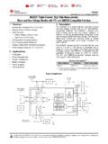
1 Product Sample & Technical Tools & Support &. Folder Buy Documents Software Community INA219 . SBOS448G AUGUST 2008 REVISED DECEMBER 2015. INA219 Zer - drift , Bidirectional Current/Power Monitor With I2C Interface 1 Features 3 Description . 1 Senses Bus Voltages from 0 to 26 V The INA219 is a current shunt and power Monitor with an I2C- or SMBUS-compatible interface. The Reports Current, Voltage, and Power device monitors both shunt voltage drop and bus 16 Programmable Addresses supply voltage, with programmable conversion times High Accuracy: (Maximum) Over and filtering. A programmable calibration value, Temperature (INA219B) combined with an internal multiplier, enables direct readouts of current in amperes. An additional Filtering Options multiplying register calculates power in watts. The Calibration Registers I2C- or SMBUS-compatible interface features 16.
2 SOT23-8 and SOIC-8 Packages programmable addresses. The INA219 is available in two grades: A and B. The 2 Applications B grade version has higher accuracy and higher Servers precision specifications. Telecom Equipment The INA219 senses across shunts on buses that can Notebook Computers vary from 0 to 26 V. The device uses a single 3- to supply, drawing a maximum of 1 mA of supply Power Management current. The INA219 operates from 40 C to 125 C. Battery Chargers Welding Equipment Device Information(1). Power Supplies PART NUMBER PACKAGE BODY SIZE (NOM). Test Equipment SOIC (8) mm mm INA219 . SOT-23 (8) mm mm (1) For all available packages, see the orderable addendum at the end of the data sheet. Simplified Schematic VS. VIN+ VIN- (Supply Voltage). INA219 . Power Register Data 2 CLK. I C-/SMBUS- Current Register Compatible Interface A0. PGA ADC. Voltage Register A1.
3 GND. 1. An IMPORTANT NOTICE at the end of this data sheet addresses availability, warranty, changes, use in safety-critical applications, intellectual property matters and other important disclaimers. PRODUCTION DATA. INA219 . SBOS448G AUGUST 2008 REVISED DECEMBER 2015 Table of Contents 1 Features .. 1 Feature 9. 2 Applications .. 1 Device Functional 11. 3 Description .. 1 12. Register Maps .. 18. 4 Revision 2. 5 Related Products .. 3 9 Application and Implementation .. 25. Application 25. 6 Pin Configuration and Functions .. 3. Typical Application .. 25. 7 4. 10 Power Supply Recommendations .. 27. Absolute Maximum Ratings .. 4. ESD 4 11 27. Layout Guidelines .. 27. Recommended Operating 4. Layout Example .. 27. Thermal Information .. 4. Electrical Characteristics:.. 5 12 Device and Documentation Support .. 28. Bus Timing Diagram 6 Community 28. Typical Characteristics.
4 7 Trademarks .. 28. Electrostatic Discharge Caution .. 28. 8 Detailed Description .. 9. Glossary .. 28. Overview .. 9. Functional Block Diagram .. 9 13 Mechanical, Packaging, and Orderable Information .. 28. 4 Revision History NOTE: Page numbers for previous revisions may differ from page numbers in the current version. Changes from Revision F (September 2011) to Revision G Page Added ESD Ratings table, Feature Description section, Device Functional Modes, Application and Implementation section, Power Supply Recommendations section, Layout section, Device and Documentation Support section, and Mechanical, Packaging, and Orderable Information section .. 1. Updated Bus Timing Diagram Definitions table. I2C timing table values were previously based on simulation and not characterized .. 6. Changes from Revision E (September 2010) to Revision F Page Changed step 5 and step 6 values in Table 26.
5 Changes from Revision D (September 2010) to Revision E Page Updated Packaging Information table .. 3. 2 Submit Documentation Feedback Copyright 2008 2015, Texas Instruments Incorporated Product Folder Links: INA219 . INA219 . SBOS448G AUGUST 2008 REVISED DECEMBER 2015. 5 Related Products DEVICE DESCRIPTION. INA209 Current/Power Monitor with watchdog, peak-hold, and fast comparator functions INA210, INA211, INA212, INA213, INA214 Zer - drift , low-cost, analog current shunt Monitor series in small package 6 Pin Configuration and Functions DCN Package 8-Pin SOT-23 D Package Top View 8-Pin SOIC. Top View IN+ 1 8 A1. A1 1 8 IN+. IN 2 7 A0. A0 2 7 IN . GND 3 6 SDA. SDA 3 6 GND. VS 4 5 SCL. SCL 4 5 VS. Pin Functions PIN. I/O DESCRIPTION. NAME SOT-23 SOIC. Analog IN+ 1 8 Positive differential shunt voltage. Connect to positive side of shunt resistor. Input Analog Negative differential shunt voltage.
6 Connect to negative side of shunt resistor. Bus voltage is IN 2 7. Input measured from this pin to ground. GND 3 6 Analog Ground VS 4 5 Analog Power supply, 3 to V. Digital SCL 5 4 Serial bus clock line Input Digital SDA 6 3 Serial bus data line I/O. Digital A0 7 2 Address pin. Table 1 shows pin settings and corresponding addresses. Input Digital A1 8 1 Address pin. Table 1 shows pin settings and corresponding addresses. Input Copyright 2008 2015, Texas Instruments Incorporated Submit Documentation Feedback 3. Product Folder Links: INA219 . INA219 . SBOS448G AUGUST 2008 REVISED DECEMBER 2015 7 Specifications Absolute Maximum Ratings over operating free-air temperature range (unless otherwise noted) (1). MIN MAX UNIT. VS Supply voltage 6 V. (2). Analog Inputs Differential (VIN+ VIN ) 26 26 V. IN+, IN Common-mode(VIN+ + VIN ) / 2 26 V. SDA GND 6 V. SCL GND VS + V.
7 Input current into any pin 5 mA. Open-drain digital output current 10 mA. Operating temperature 40 125 C. TJ Junction temperature 150 C. Tstg Storage temperature 65 150 C. (1) Stresses beyond those listed under Absolute Maximum Ratings may cause permanent damage to the device. These are stress ratings only, which do not imply functional operation of the device at these or any other conditions beyond those indicated under Recommended Operating Conditions. Exposure to absolute-maximum-rated conditions for extended periods may affect device reliability. (2) VIN+ and VIN may have a differential voltage of 26 to 26 V; however, the voltage at these pins must not exceed the range to 26 V. ESD Ratings VALUE UNIT. Human body model (HBM), per ANSI/ESDA/JEDEC JS-001, all pins (1) 4000. Electrostatic V(ESD) Charged device model (CDM), per JEDEC specification JESD22-C101, all pins (2) 750 V.
8 Discharge Machine Model (MM) 200. (1) JEDEC document JEP155 states that 500-V HBM allows safe manufacturing with a standard ESD control process. (2) JEDEC document JEP157 states that 250-V CDM allows safe manufacturing with a standard ESD control process. Recommended Operating Conditions over operating free-air temperature range (unless otherwise noted). MIN NOM MAX UNIT. VCM 12 V. VS V. TA 25 85 C. Thermal Information INA219 . THERMAL METRIC (1) D (SOIC) DCN (SOT) UNIT. 8 PINS 8 PINS. R JA Junction-to-ambient thermal resistance C/W. R JC(top) Junction-to-case (top) thermal resistance C/W. R JB Junction-to-board thermal resistance 52 C/W. JT Junction-to-top characterization parameter C/W. JB Junction-to-board characterization parameter C/W. R JC(bot) Junction-to-case (bottom) thermal resistance N/A N/A C/W. (1) For more information about traditional and new thermal metrics, see the Semiconductor and IC Package Thermal Metrics application report, SPRA953.
9 4 Submit Documentation Feedback Copyright 2008 2015, Texas Instruments Incorporated Product Folder Links: INA219 . INA219 . SBOS448G AUGUST 2008 REVISED DECEMBER 2015. Electrical Characteristics: At TA = 25 C, VS = V, VIN+ = 12V, VSHUNT = (VIN+ VIN ) = 32 mV, PGA = /1, and BRNG (1) = 1, unless otherwise noted. INA219A INA219B. PARAMETER TEST CONDITIONS UNIT. MIN TYP MAX MIN TYP MAX. INPUT. PGA = /1 0 40 0 40 mV. Full-scale current sense (input) voltage PGA = /2 0 80 0 80 mV. VSHUNT. range PGA = /4 0 160 0 160 mV. PGA = /8 0 320 0 320 mV. BRNG = 1 0 32 0 32 V. Bus voltage (input voltage) range (2). BRNG = 0 0 16 0 16 V. CMRR Common-mode rejection VIN+ = 0 to 26 V 100 120 100 120 dB. PGA = /1 10 100 10 50 (4) V. (4). PGA = /2 20 125 20 75 V. Offset voltage, RTI (3). VOS PGA = /4 30 150 30 75 (4) V. PGA = /8 40 200 40 100 (4) V. vs Temperature TA = 25 C to 85 C V/ C.
10 PSRR vs Power Supply VS = 3 to V 10 10 V/V. Current sense gain error 40 40 m%. vs Temperature TA = 25 C to 85 C 1 1 m%/ C. IN+ pin input bias current Active mode 20 20 A. IN pin input bias current || VIN pin input A ||. Active mode 20 || 320 20 || 320. impedance k . (5). IN+ pin input leakage Power-down mode A. IN pin input leakage (5) Power-down mode A. DC ACCURACY. ADC basic resolution 12 12 bits Shunt voltage, 1 LSB step size 10 10 V. Bus voltage, 1 LSB step size 4 4 mV. (. Current measurement error 4). (. over Temperature TA = 25 C to 85 C 1% 4). Bus voltage measurement error over Temperature TA = 25 C to 85 C 1% 1%. Differential nonlinearity LSB. ADC TIMING. 12 bit 532 586 532 586 s 11 bit 276 304 276 304 s ADC conversion time 10 bit 148 163 148 163 s 9 bit 84 93 84 93 s Minimum convert input low time 4 4 s SMBus SMBus timeout (6) 28 35 28 35 ms DIGITAL INPUTS (SDA as Input, SCL, A0, A1).
