Transcription of 36 V, Low Noise, Zero Drift Op Amp Data Sheet ADA4523-1
1 36 V, Low Noise, zero Drift Op Amp Data Sheet ADA4523-1 Rev. 0 Document Feedback Information furnished by Analog Devices is believed to be accurate and reliable. However, no responsibility is assumed by Analog Devices for its use, nor for any infringements of patents or other rights of third parties that may result from its use. Specifications subject to change without notice. No license is granted by implication or otherwise under any patent or patent rights of Analog Devices.
2 Trademarks and registered trademarks are the property of their respective owners. One Technology Way, Box 9106, Norwood, MA 02062-9106, Tel: 2020 Analog Devices, Inc. All rights reserved. Technical Support FEATURES Supply voltage range: V to 36 V Offset voltage: 4 V maximum at 5 V Offset voltage Drift : V/ C maximum at 5 V Input noise Voltage: 88 nV p-p from Hz to 10 Hz typical Spectral density voltage: nV/ Hz typical at 1 kHz Rail-to-rail output Unity-gain stable GBP: 5 MHz typical Slew rate: V/ s typical falling PSRR: 168 dB typical at VS = V to 36 V Open-loop voltage gain: 160 dB typical at VOUT = V to + V, RL = 10 k , VS = 30 V CMRR.
3 160 dB typical at VCM = V to + V, VS = 30 V Integrated EMI filters Shutdown mode Ground sense Available in 8-lead SOIC, 8-lead MSOP, and 8-lead LFCSP APPLICATIONS High resolution data acquisition Reference buffering Test and measurement Electronic scales Thermocouple amplifiers Strain gages Low-side current sense GENERAL DESCRIPTION The ADA4523-1 is a high voltage, low noise, zero Drift op amp that offers precision dc performance over a wide supply range of V to 36 V. Offset voltage and 1/f noise are suppressed, allowing this op amp to achieve a maximum offset voltage of 4 V and a Hz to 10 Hz input noise voltage of 88 nV p-p typical.
4 The self calibrating circuitry of the ADA4523-1 results in low offset voltage Drift with temperature ( V/ C maximum) and zero Drift over time. Additionally, the ADA4523-1 uses on-chip filtering to achieve high immunity to electromagnetic interference (EMI). Wide supply range, combined with low noise, low offset, 168 dB power supply rejection ratio (PSRR), and 160 dB common-mode rejection ratio (CMRR), make the ADA4523-1 well suited for high dynamic range test, measurement, and instrumentation systems.
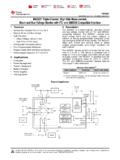
5 TYPICAL APPLICATION DIAGRAM R2750 R11k R42 FC247nFC347 FADA4523-1LT6202 VOUT8V TO TO 36V+ + C820 F(FILM)R510k FLTC6655-5 VINVOUT_FSHDN8V TO Figure 1. Precision Filtering Voltage Reference Buffer The ADA4523-1 provides a rail-to-rail output swing and an input common-mode range that includes the V rail (V V to V+ V). AD8628 LTC2057 ADA4522-1 ADA4523-1 INPUT-REFERRED VOLTAGE NOISE DENSITY (nV/ Hz)FREQUENCY (Hz) 1 10 100 1k 10k 100k110100 Figure 2. Input-Referred Voltage Noise Density vs.
6 Frequency, zero Drift Amplifier Family Comparison COMPANION PRODUCTS Voltage References: LTC6655 and ADR4525 Low Noise High Speed Amplifier: LT6202 ADC: LTC2500-32 Low Noise, Low Dropout Regulators: LT 3093 and LT3042 Additional companion products for the ADA4523-1 can be found in the Related Products section. ADA4523-1 Data Sheet Rev. 0 | Page 2 of 29 TABLE OF CONTENTS Features .. 1 Applications .. 1 General Description .. 1 Typical Application Diagram .. 1 Companion Products .. 1 Revision History .. 2 Specifications.
7 3 5 V Electrical Characteristics .. 3 30 V Electrical Characteristics .. 5 Absolute Maximum Ratings .. 7 Thermal Resistance .. 7 ESD Caution .. 7 Pin Configurations and Function Descriptions .. 8 Typical Performance Characteristics .. 10 Theory of Operation .. 20 Input Voltage Noise .. 20 Input Current Noise .. 20 Input Bias Current .. 20 Thermocouple Effects .. 21 Power 22 Electrical Overstress and Input Protection .. 23 Shutdown Mode .. 24 Applications Information .. 25 Paralleling Choppers to Improve Noise.
8 25 Solder Pad Layouts .. 26 Typical Application Circuit and Transfer Function .. 26 Related Products .. 27 Outline Dimensions .. 28 Ordering Guide .. 29 REVISION HISTORY 4/2020 Revision 0: Initial Ve r s i o n Data Sheet ADA4523-1 Rev. 0 | Page 3 of 29 SPECIFICATIONS 5 V ELECTRICAL CHARACTERISTICS TA = 25 C, supply voltage (VS) = V (V+ = + V and V = V), and common-mode voltage (VCM) = output voltage (VOUT) = 0 V, unless otherwise noted. Table 1. Parameter Symbol Test Conditions/Comments Min Typ Max Unit INPUT CHARACTERISTICS Offset Voltage1 VOS 4 V 40 C TA +125 C 5 V Offset Voltage Drift1 TCVOS 40 C TA +125 C V/ C Input Bias Current2 IB 100 300 pA 40 C TA +125 C 600 pA Input Offset Current2 IOS 200 600 pA 40 C TA +125 C 800 pA Input Voltage Range IVR 40 C TA +125 C +1 V Common-Mode Rejection Ratio CMRR VCM = V to +1 V 124 146 dB VCM = V to +1 V.
9 40 C TA +125 C 124 Input Resistance RIN Differential 47 k Common Mode 100 G Input Capacitance CIN Differential 13 pF Common Mode 20 pF Open-Loop Voltage Gain AV VOUT = V to + V, load resistance (RL) = 1 k 125 150 dB 40 C TA +125 C 125 dB OUTPUT CHARACTERISTICS Output Voltage Swing Low VOL VOL = VOUT V No load 12 20 mV No load, 40 C TA +125 C 30 mV Sink current (ISINK) = 1 mA 52 75 mV ISINK = 1 mA, 40 C TA +125 C 100 mV ISINK = 5 mA 215 300 mV ISINK = 5 mA, 40 C TA +125 C 400 mV Output Voltage Swing High VOH VOH = V+ VOUT No load 10 mV No load, 40 C TA +125 C 20 mV Source current (ISOURCE) = 1 mA 22 40 mV ISOURCE = 1 mA, 40 C TA +125 C 55 mV ISOURCE = 5 mA 106 150 mV ISOURCE = 5 mA, 40 C TA +125 C 200 mV Short-Circuit Current ISC Sourcing +25 +36 mA Sinking 25 30 mA ADA4523-1 Data Sheet Rev.
10 0 | Page 4 of 29 Parameter Symbol Test Conditions/Comments Min Typ Max Unit POWER SUPPLY Power Supply Rejection Ratio PSRR VS = V to 36 V 140 168 dB 40 C TA +125 C 140 dB Supply Current per Amplifier IS mA 40 C TA +125 C 6 mA Shutdown Amplifier Current 6 A 40 C TA +125 C A DYNAMIC PERFORMANCE Gain Bandwidth Product GBP 5 MHz Slew Rate Rising SRRISE G = 1, RL = 10 k V/ s Falling SRFA L L G = 1, RL = 10 k V/ s Internal Chopping Frequency fC 330 kHz INPUT NOISE Spectral Density Current in 1 kHz 1 pA/ Hz Voltage en 1 kHz nV/ Hz Voltage en P-P Hz to 10 Hz 88 nV p-p en RMS Hz to 10 Hz nV rms SHUTDOWN CHARACTERISTICS 40 C TA +125 C Shutdown Threshold (SD SDCOM)