Transcription of IRFZ46N - Infineon Technologies
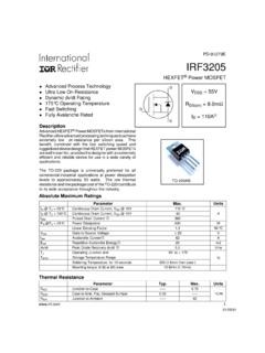
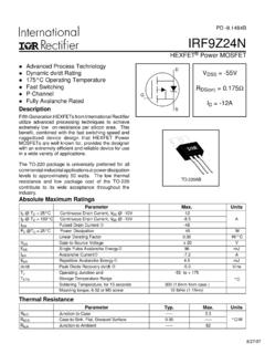
1 IRFZ46 NHEXFET Power MOSFET07/15/02 Absolute Maximum JCJunction-to-Case CSCase-to-Sink, Flat, Greased C/WR JAJunction-to-Ambient 62 Thermal = 55 VRDS(on) = ID = 53A SDGTO-220 ABAdvanced HEXFET Power MOSFETs from InternationalRectifier utilize advanced processing techniques to achieveextremely low on-resistance per silicon area. This benefit,combined with the fast switching speed and ruggedizeddevice design that HEXFET power MOSFETs are wellknown for, provides the designer with an extremely efficientand reliable device for use in a wide variety of TO-220 package is universally preferred for allcommercial-industrial applications at power dissipationlevels to approximately 50 watts.
2 The low thermalresistance and low package cost of the TO-220 contributeto its wide acceptance throughout the industry. Advanced Process Technology Ultra Low On-Resistance Dynamic dv/dt Rating 175 C Operating Temperature Fast Switching Fully Avalanche @ TC = 25 CContinuous Drain Current, VGS @ 10V 53 ID @ TC = 100 CContinuous Drain Current, VGS @ 10V37 AIDMP ulsed Drain Current 180PD @TC = 25 CPower Dissipation107 WLinear Derating CVGSGate-to-Source Voltage 20 VIARA valanche Current 28 AEARR epetitive Avalanche Energy 11mJdv/dtPeak Diode Recovery dv/dt Junction and-55 to + 175 TSTGS torage Temperature RangeSoldering Temperature, for 10 seconds300 ( from case ) CMounting torque, 6-32 or M3 srew10 lbf in ( m)PD-91277As p ParameterMin.
3 Units ConditionsISContinuous Source CurrentMOSFET symbol(Body Diode) showing theISMP ulsed Source Currentintegral reverse(Body Diode) p-n junction Forward Voltage = 25 C, IS = 28A, VGS = 0V trrReverse Recovery Time 67101nsTJ = 25 C, IF = 28 AQrrReverse Recovery Charge 208312nCdi/dt = 100A/ s tonForward Turn-On TimeIntrinsic turn-on time is negligible (turn-on is dominated by LS+LD)Source-Drain Ratings and Characteristics53180A 2 Repetitive rating; pulse width limited by max.
4 Junction temperature. ( See fig. 11 ). Starting TJ = 25 C, L = 389 H RG = 25 , IAS = 28A. (See Figure 12). ISD 228AD2di/d 2 2220A/ s, VDD2 2V(BR)DSS, TJ 175 X Pulse width 400 s; duty cycle 2%. This is a typical value at device destruction and represents operation outside rated limits. This is a calculated value limited to TJ = 175 C. Calculated continuous current based on maximum allowable junction temperature. Package limitation current is Typ. Max. Units ConditionsV(BR)DSSD rain-to-Source Breakdown Voltage55 VVGS = 0V, ID = 250 A V(BR)DSS/ TJBreakdown Voltage Temp.
5 Coefficient V/ CReference to 25 C, ID = 1mARDS(on)Static Drain-to-Source On-Resistance VGS = 10V, ID = 28A2 VGS(th)Gate Threshold = VGS, ID = 250 AgfsForward Transconductance19 SVDS = 25V, ID = 28A 25 AVDS = 55V, VGS = 0V 250 VDS = 44V, VGS = 0V, TJ = 150 CGate-to-Source Forward Leakage 100 VGS = 20 VGate-to-Source Reverse Leakage -100nAVGS = -20 VQgTotal Gate Charge 72ID = 28 AQgsGate-to-Source Charge 11nCVDS = 44 VQgdGate-to-Drain ("Miller") Charge 26 VGS = 10V, See Fig.
6 6 and 13td(on)Turn-On Delay Time 14 VDD = 28 VtrRise Time 76 ID = 28 Atd(off)Turn-Off Delay Time 52 RG = 12 tfFall Time 57 VGS = 10V, See Fig. 10 Between lead, 6mm ( )from packageand center of die contactCissInput Capacitance 1696 VGS = 0 VCossOutput Capacitance 407 VDS = 25 VCrssReverse Transfer Capacitance 110 pF = , See Fig. 5 EASS ingle Pulse Avalanche Energy 583 152 mJIAS = 28A, L = 389 HnHElectrical Characteristics @ TJ = 25 C (unless otherwise specified)LDInternal Drain InductanceLSInternal Source Inductance Leakage Currents p 4.
7 Normalized On-ResistanceVs. TemperatureFig 2. Typical Output CharacteristicsFig 1. Typical Output CharacteristicsFig 3. Typical Transfer Characteristics 1 10 100 1 10 10020 s PULSE WIDTHT = 25CJ , Drain-to-Source Voltage (V)I , Drain-to-Source Current (A) 1 10 100 1 10 10020 s PULSE WIDTHT = 175CJ , Drain-to-Source Voltage (V)I , Drain-to-Source Current (A) 1 10 100 10004567891011V = 25V20 s PULSE WIDTHDSV , Gate-to-Source Voltage (V)I , Drain-to-Source Current (A)GSDT = 25 CJ T = 175 CJ , Junction Temperature( C)R , Drain-to-Source On Resistance(Normalized)JDS(on)
8 V=I=GSD10V53As p 8. Maximum Safe Operating AreaFig 6. Typical Gate Charge VoltageFig 5. Typical Capacitance VoltageFig 7. Typical Source-Drain DiodeForward Voltage010203040506070048121620Q , Total Gate Charge (nC)V , Gate-to-Source Voltage (V)GGSFOR TEST CIRCUITSEE FIGURE I=D1328AV= 11 VDSV= 27 VDSV= 1 10 100 ,Source-to-Drain Voltage (V)I , Reverse Drain Current (A)SDSDV = 0 V GST = 25 CJ T = 175 CJ 1 10 100050010001500200025003000V , Drain-to-Source Voltage (V)C, Capacitance (pF)
9 DSVCCC====0V,CCCf = 1 MHz+ C+ CC SHORTEDGS issgsgd ,dsrssgdossdsgdCissCossCrss110100 VDS , Drain-toSource Voltage (V) , Drain-to-Source Current (A)Tc = 25 CTj = 175 CSingle Pulse1msec10msecOPERATION IN THIS AREA LIMITED BY R DS (on)100 secs p 11. Maximum Effective Transient Thermal Impedance, Junction-to-CaseFig 9. Maximum Drain Current 1 1 Notes:1. Duty factor D =t / t2. Peak T=Px Z+ T12 JDMthJCCPttDM12t , Rectangular Pulse Duration (sec)Thermal Response(Z ) = PULSE(THERMAL RESPONSE)2550751001251501750102030405060 T , Case Temperature( C)I , Drain Current (A) CDLIMITED BY PACKAGEVDS90%10%VGStd(on)trtd(off)tf h 2 2 1 h 2p 2 % h q qh q +- hhp 2IH 22 2 2 2g p 2IH 22 2 2 s p F50K.
10 2 F12 VCurrent RegulatorSame Type as Sampling Resistors+- q Fig 13b. Gate Charge Test CircuitFig 13a. Basic Gate Charge WaveformFig 12b. Unclamped Inductive WaveformsFig 12a. Unclamped Inductive Test CircuittpV(BR)DSSIASFig 12c. Maximum Avalanche EnergyVs. Drain +-VDDDRIVERA15V20V2550751001251501750501 00150200250300350 Starting T , Junction Temperature( C)E , Single Pulse Avalanche Energy (mJ)JAS IDTOPBOTTOM11A 20A 28A s p 2h 2 2 G 2 2g Recoverydv/dtRipple 5%Body Diode Forward DropRe-AppliedVoltageReverseRecoveryCurr entBody Diode ForwardCurrentVGS=10 VVDDISDD river Gate VDSW aveformInductor CurentD = P.