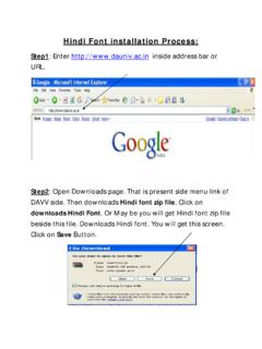
Transcription of Lesson-12: MOSFET (enhancement and depletion mode ...
1 2008 EDCL esson12-" , Raj Kamal, 1 EDC Lesson 12: Transistor and FET CharacteristicsLessonLesson--12: 12: MOSFET ( enhancement MOSFET ( enhancement and depletion mode) Characteristics and depletion mode) Characteristics and Symbolsand Symbols2008 EDCL esson12-" , Raj Kamal, 21. Metal Oxide Semiconductor Field Effect 1. Metal Oxide Semiconductor Field Effect Transistor ( MOSFET )Transistor ( MOSFET )2008 EDCL esson12-" , Raj Kamal, 3 Types of FETsTypes of FETsThe family of FETs may be divided into: Junction FET depletion Mode MOSFET enhancement Mode MOSFET2008 EDCL esson12-" , Raj Kamal, 4 Remember JFET Definition JFET is a unipolar-transistor, which acts as a voltage controlled current device and is a device in which current at two electrodes is controlled by the action of an electric field at a reversed biased p-n " , Raj Kamal, 5 MOSFET Definition MOSFET Field effect transistor is a unipolar-transistor, which acts as a voltage-controlled current device and is a device in which current at two electrodes drain and source is controlled by the action of an electric field at another electrode gate having in-between semiconductor and metal very a thin metal oxide layer.
2 2008 EDCL esson12-" , Raj Kamal, 6nn--channel depletion channel depletion MetalMetal--OxideOxide--Semiconductor FET ( MOSFET )Semiconductor FET ( MOSFET )n channelp2008 EDCL esson12-" , Raj Kamal, 7pp--channel depletion channel depletion MetalMetal--OxideOxide--Semiconductor FET ( MOSFET )Semiconductor FET ( MOSFET )p channeln 2008 EDCL esson12-" , Raj Kamal, 8 Effect of Insulating SiO2(metal-oxide) layer MOSFET Very high input impedance due to SiO2layer compared to even reverse biased p-n junction depletion region input impedance in JFET2008 EDCL esson12-" , Raj Kamal, 9nn--channel depletion regionchannel depletion region2008 EDCL esson12-" , Raj Kamal, 10nn--channel depletion region (normally ON)channel depletion region (normally ON)2008 EDCL esson12-" , Raj Kamal, 11 Transfer Characteristics of nTransfer Characteristics of n--channel channel depletion region MOSFET depletion region MOSFET2008 EDCL esson12-" , Raj Kamal, 12 There is a convenient relationship between IDSand VGS.
3 Beyond pinch-off Where IDSSis drain current when VGS= 0 and VGS(off)is defined as VP, that is gate-source voltage that just pinches off the channel. The pinch off voltage VPhere is a +ve quantity because it was introduced through VDS(sat). VGS(off)however is negative, )(1 offGSGSDSSDSVVII2008 EDCL esson12-" , Raj Kamal, 13pp--channel depletion MOSFET channel depletion MOSFET2008 EDCL esson12-" , Raj Kamal, 14pp--channel depletion MOSFET (Normally ON at channel depletion MOSFET (Normally ON at VGS = 0)VGS = 0)2008 EDCL esson12-" , Raj Kamal, 152. enhancement Mode MOSFETS2. enhancement Mode MOSFETS2008 EDCL esson12-" , Raj Kamal, 16nn--channel enhancement mode MOSFET channel enhancement mode MOSFET2008 EDCL esson12-" , Raj Kamal, 17nn--channel enhancement mode Normally Offchannel enhancement mode Normally Off2008 EDCL esson12-" , Raj Kamal, 18 Note that with a n-channel device we apply a +ve gate voltage to allow source-drain current, with a p-channel device we apply a -ve gate enhancement modep-channel enhancement mode2008 EDCL esson12-" , Raj Kamal, 19pp--channel enhancement MOSFET channel enhancement MOSFET2008 EDCL esson12-" , Raj Kamal, 20pp--channel enhancement MOSFET (normally channel enhancement MOSFET (normally OFF)OFF)2008 EDCL esson12-" , Raj Kamal, 213.
4 enhancement Mode mosfets in detail 3. enhancement Mode mosfets in detail 2008 EDCL esson12-" , Raj Kamal, 22 Basic MOSFET (nBasic MOSFET (n--channel) enhancement modechannel) enhancement modeWhen VGS = 0, the n-channel is very thin and channel width enhances with+ VGS2008 EDCL esson12-" , Raj Kamal, 23 Channel width enhancement with +VChannel width enhancement with +VGSGS The gate electrode is placed on top of a very thin insulating layer. There are a pair of small n-type regions just under the drain & source electrodes. If apply a +ve voltage to gate, will push away the holes inside the p-type substrate and attracts the moveable electrons in the n-type regions under the source & drain " , Raj Kamal, 24 enhancement mode MOSFET Increasing the +ve gate voltage pushes the p-type holes further away and enlarges the thickness of the created channel. As a result increases the amount of current which can go from source to drain this is why this kind of transistor is called an enhancement modeMOSFET.
5 2008 EDCL esson12-" , Raj Kamal, 25 Subthreshold region in nSubthreshold region in n--chennel enhancement mode chennel enhancement mode ID= k exp (qVGS/kBT) where T temperature iu in Kelvin, is Boltzman constant 2008 EDCL esson12-" , Raj Kamal, 26 Subthreshold region in nSubthreshold region in n--chennel enhancement mode chennel enhancement mode ID= k (VGS VT)22008 EDCL esson12-" , Raj Kamal, 27 Above Threshold Above Threshold ON stateON stateID= k (VGS VT)2 = (VGS VT)2 mA015432876 IDVGSIf ID(on) = 10 mA and VGS = 8 V, then k =10 mA/(8V 2V)2= mA/V2VT = 2 V2008 EDCL esson12-" , Raj Kamal, 28 Above Threshold Above Threshold ON stateON stateID= k (VGS VT)2 = (VGS VT)2 mAIf ID(on) = 10 mA and VGS = 8 V, then k =10 mA/(8V 2V)2= mA/V2VT = 2 VID= k (VGS VT)22008 EDCL esson12-" , Raj Kamal, 29 Ideal Output Characteristics of MOSFETI deal Output Characteristics of MOSFET2008 EDCL esson12-" , Raj Kamal, 30 Ideal Output linear region before saturation Ideal Output linear region before saturation Characteristics of MOSFETC haracteristics of MOSFET2008 EDCL esson12-" , Raj Kamal, 31 Ideal Output Saturation formula of enhancement Ideal Output Saturation formula of enhancement mode MOSFET mode MOSFET chang2008 EDCL esson12-" , Raj Kamal, 32 Transfer Characteristics in above threshold region Transfer Characteristics in above threshold region and saturation region in nand saturation region in n--channel enhancement channel enhancement modemode7 V6 V5 V4 V3 VVGS=VT = 2V2008 EDCL esson12-" , Raj Kamal.
6 33 Transfer Characteristics in Subthreshold region and Transfer Characteristics in Subthreshold region and saturation region in nsaturation region in n--channel enhancement modechannel enhancement mode2008 EDCL esson12-" , Raj Kamal, 344. Symbols of depletion and enhancement 4. Symbols of depletion and enhancement Mode MOSFETSMode MOSFETS2008 EDCL esson12-" , Raj Kamal, 35 Symbol of depletion mode mosfets ymbol of depletion mode MOSFETn-channel depletion Mode MOSFETp-channel depletion Mode MOSFET 2008 EDCL esson12-" , Raj Kamal, 36 Symbol of enhancement mode of mosfets ymbol of enhancement mode of MOSFETn-channel enhancement Mode MOSFETp=channel enhancement Mode MOSFET 2008 EDCL esson12-" , Raj Kamal, 37 SummarySummary2008 EDCL esson12-" , Raj Kamal, 38We learnt Definitions of MOSFET n-channel and p-channel depletion MOSFET normally ON, Pinch off on VGS in n- MOSFET and + VGS in p- MOSFET n-channel and p-channel enhancement MOSFET normally OFF, below Threshold and above VT on + VGS in n- MOSFET and -VGS in p-MOSFET2008 EDCL esson12-" , Raj Kamal, 39 End of Lesson 12 End of Lesson 12