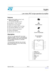
Transcription of LF411 JFET-INPUT OPERATIONAL AMPLIFIER - TI.com
1 LF411 JFET-INPUT OPERATIONAL AMPLIFIER SLOS011C MARCH 1987 REVISED OCTOBER 19971 POST OFFICE BOX 655303 DALLAS, TEXAS 75265 DLow Input Bias Current, 50 pA TypDLow Input noise Current, pA/ Hz TypDLow Supply Current, 2 mA TypDHigh Input impedance, 1012 TypDLow Total Harmonic DistortionDLow 1/f noise Corner, 50 Hz TypDPackage Options Include PlasticSmall-Outline (D) and Standard (P) DIPs descriptionThis device is a low-cost, high-speed, JFET-INPUT OPERATIONAL AMPLIFIER with very low input offset voltage anda maximum input offset voltage drift . It requires low supply current, yet maintains a large gain-bandwidth productand a fast slew rate. In addition, the matched high-voltage JFET input provides very low input bias and LF411 can be used in applications such as high-speed integrators, digital-to-analog converters,sample-and-hold circuits, and many other LF411C is characterized for operation from 0 C to 70 C.
2 The LF411I is characterized for operation from 40 C to 85 +IN IN +OUTBAL1 BAL223156 AVAILABLE OPTIONSVIOmaxPACKAGETAVIOmaxAT 25 CSMALL OUTLINE(D)PLASTIC DIP(P)0 C to 70 C2 mVLF411 CDLF411CP 40 C to 85 C2 mVLF411 IDLF411 IPThe D packages are available taped and reeled. Add the suffix R to thedevice type ( , LF411 CDR).Copyright 1997, Texas Instruments IncorporatedPRODUCTION DATA information is current as of publication conform to specifications per the terms of Texas Instrumentsstandard warranty. Production processing does not necessarily includetesting of all parameters. 12348765 BAL1IN IN +VCC NCVCC +OUTBAL2D OR P PACKAGE(TOP VIEW)NC No internal connectionPlease be aware that an important notice concerning availability, standard warranty, and use in critical applications ofTexas Instruments semiconductor products and disclaimers thereto appears at the end of this data OPERATIONAL AMPLIFIER SLOS011C MARCH 1987 REVISED OCTOBER 19972 POST OFFICE BOX 655303 DALLAS, TEXAS 75265absolute maximum ratings over operating free-air temperature range (unless otherwise noted)Supply voltage, VCC + 18 V.
3 Supply voltage, VCC 18 V.. Differential input voltage, VID 30 V.. Input voltage, VI (see Note 1) 15 V.. Duration of output short circuit Unlimited.. Continuous total power dissipation 500 mW.. Package thermal impedance, JA (see Note 2): D package197 C/W.. P package104 C/W.. Storage temperature range, Tstg 65 C to 150 C.. Lead temperature 1,6 mm (1/16 inch) from case for 10 seconds 260 C.. NOTES: 1. Unless otherwise specified, the absolute maximum negative input voltage is equal to the negative power supply The package thermal impedance is calculated in accordance with JESD 51, except for through-hole packages, which use a tracelength of operating conditionsC SUFFIXI SUFFIXUNITMINMAXMINMAXUNITS upply voltage, VCC + voltage, VCC 18 18 VOperating free-air temperature, TA070 40 85 Celectrical characteristics over operating free-air temperature range, VCC = 15 V (unless otherwisespecified)
4 PARAMETERTEST CONDITIONSTAMINTYPMAXUNITPARAMETERTEST CONDITIONSLF411 CLF411 IMINTYPMAXUNITVIOI nput offset voltageVIC = 0,RS = 10 k 25 C25 VIOA verage temperature coeffi-cient of input offset voltageVIC = 0,RS = 10 k 1020 V/ CIIOInp t offset c rrent VIC=025 C25 C25100pAIIOI nput offset current VIC = 070 C85 C2nAIIBInp t bias c rrent VIC=025 C25 C50200pAIIBI nput bias current VIC = 070 C85 C4nAVICRC ommon-mode input voltagerange 11 peak output-voltageswingRL = 10 k 12 differential VO= 10 VRL=2k 25 C25 C25200V/mVAVD ggvoltageVO = 10 V,RL = 2 k 0 C to 70 C 40 C to 85 C15200V/mVriInput resistanceTJ = 25 C1012 CMRRC ommon-mode rejection ratioRS 10 k 70100dBkSVRS upply-voltage rejection ratioSee Note 370100dBICCS upply At least 90% of the devices meet this limit for VIO.
5 Input bias currents of an FET-input OPERATIONAL AMPLIFIER are normal junction reverse currents, which are temperature sensitive. Pulse techniquesmust be used that will maintain the junction temperatures as close to the ambient temperature as 3: Supply-voltage rejection ratio is measured for both supply magnitudes increasing or decreasing OPERATIONAL AMPLIFIER SLOS011C MARCH 1987 REVISED OCTOBER 19973 POST OFFICE BOX 655303 DALLAS, TEXAS 75265operating characteristics, VCC = 15 V, TA = 25 CPARAMETERTEST CONDITIONSMINTYPMAXUNITSRSlew rate813V/ sB1 Unity-gain input noise voltagef = 1 kHz,RS = 20 18nV/ HzInEquivalent input noise currentf = 1 HzPACKAGE OPTION 1 PACKAGING INFORMATIONO rderable DeviceStatus(1)Package TypePackageDrawingPinsPackageQtyEco Plan(2)Lead finish/Ball material(6)MSL Peak Temp(3)Op Temp ( C)Device Marking(4/5)
6 SamplesLF411 CDACTIVESOICD875 RoHS & GreenNIPDAUL evel-1-260C-UNLIM0 to 70LF411 CLF411 CDRACTIVESOICD82500 RoHS & GreenNIPDAUL evel-1-260C-UNLIM0 to 70LF411 CLF411 CDRG4 ACTIVESOICD82500 RoHS & GreenNIPDAUL evel-1-260C-UNLIM0 to 70LF411 CLF411 CPACTIVEPDIPP850 RoHS & GreenNIPDAUN / A for Pkg Type0 to 70LF411 CPLF411 CPE4 ACTIVEPDIPP850 RoHS & GreenNIPDAUN / A for Pkg Type0 to 70LF411CP (1) The marketing status values are defined as follows:ACTIVE: Product device recommended for new : TI has announced that the device will be discontinued, and a lifetime-buy period is in : Not recommended for new designs. Device is in production to support existing customers, but TI does not recommend using this part in a new : Device has been announced but is not in production.
7 Samples may or may not be : TI has discontinued the production of the device. (2) RoHS: TI defines "RoHS" to mean semiconductor products that are compliant with the current EU RoHS requirements for all 10 RoHS substances, including the requirement that RoHS substancedo not exceed by weight in homogeneous materials. Where designed to be soldered at high temperatures, "RoHS" products are suitable for use in specified lead-free processes. TI mayreference these types of products as "Pb-Free".RoHS Exempt: TI defines "RoHS Exempt" to mean products that contain lead but are compliant with EU RoHS pursuant to a specific EU RoHS : TI defines "Green" to mean the content of Chlorine (Cl) and Bromine (Br) based flame retardants meet JS709B low halogen requirements of <=1000ppm threshold.
8 Antimony trioxide basedflame retardants must also meet the <=1000ppm threshold requirement. (3) MSL, Peak Temp. - The Moisture Sensitivity Level rating according to the JEDEC industry standard classifications, and peak solder temperature. (4) There may be additional marking, which relates to the logo, the lot trace code information, or the environmental category on the device. (5) Multiple Device Markings will be inside parentheses. Only one Device Marking contained in parentheses and separated by a "~" will appear on a device. If a line is indented then it is a continuationof the previous line and the two combined represent the entire Device Marking for that device. (6) Lead finish/Ball material - Orderable Devices may have multiple material finish options.
9 Finish options are separated by a vertical ruled line. Lead finish/Ball material values may wrap to twolines if the finish value exceeds the maximum column width. PACKAGE OPTION 2 Important Information and Disclaimer:The information provided on this page represents TI's knowledge and belief as of the date that it is provided. TI bases its knowledge and belief on informationprovided by third parties, and makes no representation or warranty as to the accuracy of such information. Efforts are underway to better integrate information from third parties. TI has taken andcontinues to take reasonable steps to provide representative and accurate information but may not have conducted destructive testing or chemical analysis on incoming materials and and TI suppliers consider certain information to be proprietary, and thus CAS numbers and other limited information may not be available for release.
10 In no event shall TI's liability arising out of such information exceed the total purchase price of the TI part(s) at issue in this document sold by TI to Customer on an annual basis. TAPE AND REEL INFORMATION*All dimensions are nominalDevicePackageTypePackageDrawingPi nsSPQReelDiameter(mm)ReelWidthW1 (mm)A0(mm)B0(mm)K0(mm)P1(mm)W(mm) MATERIALS Materials-Page 1*All dimensions are nominalDevicePackage TypePackage DrawingPinsSPQL ength (mm)Width (mm)Height (mm) MATERIALS Materials-Page 2 TUBE*All dimensions are nominalDevicePackage NamePackage TypePinsSPQL (mm)W (mm)T ( m)B (mm) MATERIALS Materials-Page TYP[ ].069 MAX[ ] 6X .050[ ]8X . [ ] [ ]. TYP[ ]0- [ ].010[ ]. [ ]4X (0-15) [ ]NOTE [ ]NOTE 44X (0-15)(.041)[ ]SOIC - mm max heightD0008 ASMALL OUTLINE INTEGRATED CIRCUIT4214825/C 02/2019 NOTES: 1.