Transcription of Low-Power, Single-Supply, CMOS Instrumentation …
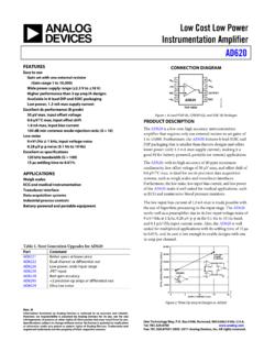
1 INA331 INA2331 SBOS215C DECEMBER 2001 REVISED APRIL 2005 DESCRIPTIONThe INA331 and INA2331 are rail-to-rail output, low-powerCMOS Instrumentation amplifiers that offer wide range, single-supply operation as well as bipolar-supply operation. TheINA331 family provides low-cost, low-noise amplification ofdifferential signals with a low quiescent current of 415 A(dropping to A when shutdown). Returning to normaloperation within microseconds, this INA can be used forbattery or multi-channel internally in a gain of 5V/V, the INA331 offersflexibility in higher gains by choosing external DESIGNED FOR LOW COST HIGH GAIN ACCURACY: G = 5, , 2ppm/ C GAIN SET WITH EXT.
2 RESISTORS FOR > 5V/V LOW OFFSET VOLTAGE: 250 V HIGH CMRR: 94dB DC, 50dB at 45kHz LOW BIAS CURRENT: BANDWIDTH, SLEW RATE: , 5V/ s RAIL-TO-RAIL OUTPUT SWING: (V+) WIDE TEMPERATURE RANGE: 55 C to +125 C LOW QUIESCENT CURRENT: 490 A max/chan SHUT DOWN: A MSOP-8 SINGLE AND TSSOP-14 DUAL PACKAGESC opyright 2001-2005, Texas Instruments IncorporatedLow- power , Single-Supply, CMOSINSTRUMENTATION AMPLIFIERSP lease be aware that an important notice concerning availability, standard warranty, and use in critical applications ofTexas Instruments semiconductor products and disclaimers thereto appears at the end of this data INDUSTRIAL SENSOR AMPLIFIERS:Bridge, RTD, Thermocouple, Position PHYSIOLOGICAL AMPLIFIERS.
3 ECG, EEG, EMG A/D CONVERTER SIGNAL CONDITIONING DIFFERENTIAL LINE RECEIVERS WITH GAIN FIELD UTILITY METERS PCMCIA CARDS AUDIO AMPLIFIERS COMMUNICATION SYSTEMS TEST EQUIPMENT AUTOMOTIVE INSTRUMENTATIONThe INA331 rejects line noise and its harmonics, becausecommon-mode error remains low even at higher bandwidth and slew rate makes the INA331 ideal fordirectly driving sampling Analog-to-Digital (A/D) convertersas well as general-purpose high precision, low cost, and small packages, theINA331 outperforms discrete designs. They are specified fora wide temperature range of 55 C to +125 VREFVIN VIN+10k 10k ShutdownV+VOUTG = 5 + (5R2/R1)V R2R1RG40k Ch AINA2331 INA331Ch B INA2331 INA331 PRODUCTION DATA information is current as of publication conform to specifications per the terms of Texas Instrumentsstandard warranty.
4 Production processing does not necessarily includetesting of all trademarks are the property of their respective , Voltage, V+ to V .. Input Terminals, Voltage(2).. (V ) to (V+) + (2).. 10mAOutput Short-Circuit(3).. ContinuousOperating Temperature .. 55 C to +125 CStorage Temperature .. 65 C to +150 CJunction Temperature .. 150 CLead Temperature (soldering, 10s) .. 300 CNOTES: (1) Stresses above these ratings may cause permanent to absolute maximum conditions for extended periods may degradedevice reliability. (2) Input terminals are diode-clamped to the power -supply signals that can swing more than beyond the supply rails should becurrent limited to 10mA or less.
5 (3) Short-circuit to ground, one amplifier MAXIMUM RATINGS(1)ELECTROSTATICDISCHARGE SENSITIVITYThis integrated circuit can be damaged by ESD. Texas Instru-ments recommends that all integrated circuits be handled withappropriate precautions. Failure to observe proper handlingand installation procedures can cause damage can range from subtle performance degradationto complete device failure. Precision integrated circuits may bemore susceptible to damage because very small parametricchanges could cause the device not to meet its CONFIGURATIONTop ViewRGVIN VIN+V ShutdownV+VOUTREFINA331 MSOP-8 (DGK)123487651234567141312111098 Shutdown AVOUTAREFAV+REFBVOUTBS hutdown BRGAVIN AVIN+AV VIN+BVIN BRGBINA2331 Dual, TSSOP-14 (PW)PACKAGEPACKAGEPRODUCTPACKAGE-LEADDES IGNATORMARKINGS ingleINA331 IDGKMSOP-8 DGKC31 INA331 AIDGKMSOP-8 DGKC31 DualINA2331 AIPWTSSOP-14PW2331 ANOTES.
6 (1) For the most current package and ordering information, see the Package Option Addendum at the end of this document, or see the TI website INFORMATION(1)INA331, CHARACTERISTICS: VS = + to + limits apply over the specified temperature range, TA = 55 C to 125 TA = +25 C, RL = 10k , G = 25, and VREF = VS/2, unless otherwise Offset Voltage, RTIVS = +5V 250 500 1000 VOver TemperatureVOS CoefficientdVOS/dT 5 V/ Cvs power SupplyPSRRVS = + to + 50 200 V/Vvs Temperature 220 V/VLong-Term Stability V/monthInput Impedance1013 || 3 || pFInput Common-Mode RangeVS = VVS = VCommon-Mode RejectionCMRRVS = 5V, VCM = to dB 40 C to +85 CVS = 5V, VCM = to TemperatureVS = 5V, VCM = to =.
7 VCM = to dBCrosstalk, Dual114dBINPUT BIAS CURRENTVCM = VS/2 Bias Current IB 10 pAOffset Current IOS 10 pANOISE, RTIRS = 0 Voltage Noise: f = 10 HzeN280 nV/ Hzf = 100Hz96 nV/ Hzf = 1kHz46 nV/ Hzf = to 10Hz7 VPPC urrent Noise: f = fA/ HzGAIN(1)Gain Equation, Externally SetG > 5G = 5 + (5R2/R1) Range of Gain51000 V/VGain ErrorG = 5 %vs TemperatureG = 5 2 10 ppm/ CNonlinearityG = 25(2), VS = 5V, VO = to % of FSOver Temperature % of FSOUTPUTO utput Voltage Swing from Rail(3)RL = 10k 5025 mVOver TemperatureG > 1050 mVCapacitance Load DriveSee Typical Characteristics pFShort-Circuit Current+48/ 32 mAFREQUENCY RESPONSEB andwidth, 3dBBWG = MHzSlew RateSRVS = 5V, G = 255 V/ sSettling Time, = 25, CL = 100pF, VO = 2V sOverload Recovery50% Input Overload G = 252 sPOWER SUPPLYS pecified Voltage Range+ + VOperating Voltage Range+ to + VQuiescent Current per ChannelIQVSD > (3)415490 AOver Temperature600 AShutdown Quiescent Current/ChanISDVSD < (3)
8 ATEMPERATURE RANGES pecified/Operating Range 55+125 CStorage Range 65+150 CThermal Resistance JAMSOP-8, TSSOP-14 Surface Mount150 C/W Specifications same as INA331 IDGKNOTES: (1) Does not include errors from external gain setting resistors.(2) Output voltage swings are measured between the output and power -supply rails. Output swings to rail only if G 10. Output does not swing to positiverail if gain is less than 10.(3) See typical characteristic Percent Overshoot vs Load Capacitance.(4) See typical characteristic Shutdown Voltage vs Supply , CHARACTERISTICSAt TA = +25 C, VS = 5V, VCM = VS/2, RL = 10k , and CL = 100pF, unless otherwise vs FREQUENCY10 Gain (dB)Frequency (Hz)1001k10k100k1M10M80706050403020100 10 20 Gain = 500 Gain = 100 Gain = 25 Gain = 5 COMMON-MODE REJECTION RATIO vs FREQUENCY10 CMRR (dB)Frequency (Hz)1001k10k100k120100806040200 power -SUPPLY REJECTION RATIOvs FREQUENCY1 PSRR (dB)Frequency (Hz)101001k10k100k1009080706050403020100 MAXIMUM OUTPUT VOLTAGE vs FREQUENCY100 Maximum Output Voltage (VPP)Frequency (Hz)
9 1k10k100k1M10M6543210VS = = = vs FREQUENCY1 VNOISE (nV/ Hz)INOISE (fA/ Hz)Frequency (Hz) TO 10Hz VOLTAGE NOISE1s/div2 V/divINA331, CHARACTERISTICS (Cont.)At TA = +25 C, VS = 5V, VCM = VS/2, RL = 10k , and CL = 100pF, unless otherwise INPUT RANGEvs REFERENCE VOLTAGE0 Output Referred to Ground (V)Input Common-Mode Voltage (V)123456543210 Outside of Normal OperationREFI ncreasingQUIESCENT CURRENT AND SHUTDOWN CURRENTvs power SUPPLYIQ ( A), ISD (nA)Supply Voltage (V) CURRENT vs power SUPPLYISC (mA)Supply Voltage (V) +ISC SHORT-CIRCUIT CURRENT vs TEMPERATUREISC (mA)Temperature ( C) 7525 50 25050751001251506050403020100 ISC+ISC OUTPUT SWING vs LOAD RESISTANCES wing-to-Rail (mV)RLOAD ( )
10 010k20k30k40k50k2520151050To Positive RailTo Negative RailQUIESCENT CURRENT AND SHUTDOWN CURRENT vs TEMPERATUREIQ ( A)Temperature ( C) 75 50 2502550751001251506005505004504003503002 50200150100500 IQISDINA331, CHARACTERISTICS (Cont.)At TA = +25 C, VS = 5V, VCM = VS/2, RL = 10k , and CL = 100pF, unless otherwise STEP RESPONSE (G = 5)4 s/div100mV/divSMALL-SIGNAL STEP RESPONSE (G = 100)4 s/div50mV/divSMALL-SIGNAL STEP RESPONSE (G = 5, CL = 1000pF)4 s/div100mV/divSMALL-SIGNAL STEP RESPONSE (G = 100, CL = 1000pF)10 s/div50mV/divSMALL-SIGNAL STEP RESPONSE (G = 100, CL = 4700pF)10 s/div50mV/divLARGE-SIGNAL STEP RESPONSE (G = 25)10 s/div1V/divINA331, CHARACTERISTICS (Cont.)