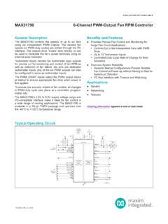
Transcription of MAX9611/MAX9612 - High-Side, Current-Sense Amplifiers …
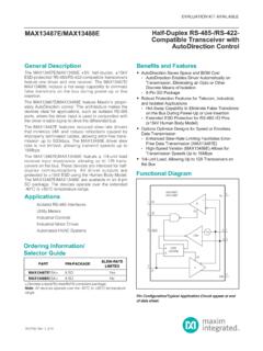
1 General DescriptionThe MAX9611/MAX9612 are high - side Current-Sense Amplifiers with an integrated 12-bit ADC and a gain block that can be configured either as an op amp or comparator, making these devices ideal for a number of industrial and automotive high - side , Current-Sense Amplifiers operate over a wide 0V to 60V input common-mode voltage range. The programmable full-scale voltage (440mV, 110mV, and 55mV) of these Amplifiers offers wide dynamic range, accurate current measurement, and application flexibility in choosing sense resistor values. A choice of either an internal op amp or a comparator is provided to the user . The internal amplifier can be used to limit the inrush cur-rent or to create a current source in a closed-loop system.
2 The comparator can be used to monitor fault events for fast I2C-controlled 12-bit, 500sps analog-to-digital con-verter (ADC) can be used to read the voltage across the sense resistor (VSENSE), the input common-mode voltage (VRSCM), op-amp/comparator output (VOUT), op-amp/comparator reference voltage (VSET), and internal die temperature. The I2C bus is compatible with and logic, allowing modern microcontrollers to interface to MAX9611 features a noninverting input-to-output configuration while the MAX9612 features an inverting input-to-output MAX9611/MAX9612 operate with a to supply voltage range, are fully specified over the -40 C to +125 C automotive temperature range, and are available in a 3mm x 5mm, 10-pin MAX Hybrid Automotive Power Supplies Server Backplanes Base-Station PA Control Base-Station Feeder Cable Bias-T Telecom Cards Battery-Operated EquipmentFeatures 0V to +60V Input Common-Mode Voltage Range to Power-Supply Range.
3 Compatible with and Logic 5 A Software Shutdown current Integrated 12-Bit ADC 13 V Current-Sense ADC Resolution 500 V (max) Current-Sense ADC Input Offset Voltage (max) Current-Sense ADC Gain Error I2C Bus with 16 Addresses Small, 3mm x 5mm 10-Pin MAX Package -40 C to +125 C Operating Temperature RangeFunctional Diagrams appear at end of data ; Rev 5; 12/19 MAX is a registered trademark of Maxim Integrated Products, here for production status of specific part : All devices operate over the -40 C to +125 C tempera-ture range. +Denotes a lead(Pb)-free/RoHS-compliant package. PARTOUTPUTPIN-PACKAGEMAX9611 AUB+Noninverting10 MAXMAX9612 AUB+Inverting10 MAXO rdering Information/Selector GuideTypical Application CircuitMAX9611 MAX9612 VCC LOGICSCLSDARS+ FVIN0V TO 60 VLOADRSENSEMAX9611/MAX9612 high - side , Current-Sense Amplifiers with12-Bit ADC and Op Amp/ComparatorEVALUATION KIT AVAILABLEVCC to GND.
4 To +6 VRS+, RS-, OUT to GND .. to +65 VDifferential Input Voltage, RS+ - RS- .. 65 VAll Other Pins to GND .. to +6 VOUT Short-Circuit to GND ..ContinuousContinuous current into Any Pin .. 20mAContinuous Power Dissipation (TA = +70 C) 10-Pin MAX (derate C above +70 C) ..707mW MAX Package Junction-to-Ambient Thermal Resistance ( JA) (Note 1) ..13 C/WOperating Temperature Range ..-40 C to +125 CJunction Temperature ..+150 CStorage Temperature Range ..-65 C to +150 CLead Temperature (soldering, 10s) ..+300 CSoldering Temperature (reflow) ..+260 C(VCC = , VRS+ = VRS- = +12V, VSENSE = (VRS+ - VRS-) = 0V, TA = -40 C to +125 C, unless otherwise noted. Typical values are at TA = +25 C.)
5 (Note 2)PARAMETERSYMBOLCONDITIONSMINTYPMAXUNIT SCURRENT-SENSE amplifier DC CHARACTERISTICSI nput Common-Mode RangeGuaranteed by CMRR060 VInput Offset Voltage ADC Path (Note 3)VOSTA = +25 C, gain = = -40 C to +125 C, gain = 8x2TA = +25 C, gain = = -40 C to +125 C, gain = 4x2TA = +25 C, gain = = -40 C to +125 C, gain = Error (Note 3)GETA = +25 C, gain = = -40 C to + 85 C, gain = = -40 C to +125 C, gain = = +25 C, gain = = -40 C to +125 C, gain = = +25 C, gain = 1x14TA = -40 C to +125 C, gain = Input ResistanceRINDM300k Common-Mode Input ResistanceRINCM12M Input Bias CurrentIRS+, IRS-TA = +25 C12 ATA = -40 C to +125 C5 Input Offset current (Note 4)(IRS+) - (IRS-)TA = +25 C36nATA = -40 C to +125 C6 Note 1: Package thermal resistances were obtained using the method described in JEDEC specification JESD51-7, using a four-layer board.
6 For detailed information on package thermal considerations, refer to Maximum RatingsStresses beyond those listed under Absolute Maximum Ratings may cause permanent damage to the device. These are stress ratings only, and functional operation of the device at these or any other conditions beyond those indicated in the operational sections of the specifications is not implied. Exposure to absolute maximum rating conditions for extended periods may affect device CharacteristicsMAX9611/MAX9612 high - side , Current-Sense Amplifiers with12-Bit ADC and Op Integrated 2(VCC = , VRS+ = VRS- = +12V, VSENSE = (VRS+ - VRS-) = 0V, TA = -40 C to +125 C, unless otherwise noted. Typical values are at TA = +25 C.)
7 (Note 2)PARAMETERSYMBOLCONDITIONSMINTYPMAXUNIT SC ommon-Mode Rejection RatioCMRRVRS- = 0V to 60V,TA = +25 CGain = 8x, VSENSE = 50mV106120dBGain = 4x, VSENSE = 100mV106120 Gain = 1x, VSENSE = 400mV100120 VRS- = 0V to 60V,TA = -40 C to +125 CGain 8x, VSENSE = 50mV94 Gain 4x, VSENSE = 100mV94 Gain 1x, VSENSE = 400mV84 Power-Supply Rejection RatioPSRR VCC = to = 8x, VSENSE = 50mV5772dBGain = 4x, VSENSE = 100mV5667 Gain = 1x, VSENSE = 400mV4857 Full-Scale Sense VoltageFSUsed in gain error measurementGain = 8x55mVGain = 4x110 Gain = 1x440 LSB Step SizeLSBGain = VGain = = PATH, CSA + amplifier /COMPARATORI nput Offset VoltageVOSTA = +25 = -40 C to +125 C10 SET Input Bias CurrentIB150nAMaximum SET Input Voltage Range BandwidthBWGain = 1x, RS- = 4 MHzGain DelaytPDIn comparator mode, 10mV sInternal HysteresisVHYSIn comparator mode, nonlatching8mVOutput Sink CurrentVOUT = 4V15mAOutput Leakage CurrentVOUT = AOutput Voltage LowVOLISINK = 8mA, TA = -40 C to +85 C1 VISINK = 8mA, TA = -40 C to +125 Characteristics (continued) MAX9611/MAX9612 high - side , Current-Sense Amplifiers with12-Bit ADC and Op Integrated 3(VCC = , VRS+ = VRS- = +12V, VSENSE = (VRS+ - VRS-) = 0V, TA = -40 C to +125 C, unless otherwise noted.)
8 Typical values are at TA = +25 C.) (Note 2)PARAMETERSYMBOLCONDITIONSMINTYPMAXUNIT SOUT VOLTAGE MEASUREMENT (VOUT)Full-Scale Input Step SizeLSB14mVGain ErrorGEVRSCM = (VRS+ - VRS-)/2TA = +25 = -40 C to +125 C7 Input Offset VoltageVOSOUTTA = +25 C14110mVTA = -40 C to +125 C160 COMMON-MODE VOLTAGE MEASUREMENT (VRSCM)Full-Scale Input Step SizeLSB14mVGain ErrorGEVRSCM = (VRS+ - VRS-)/2TA = +25 = -40 C to +125 C7 Input Offset VoltageVOSOUTTA = +25 C1480mVTA = -40 C to +125 C160 SET VOLTAGE MEASUREMENT (VSET)Full-Scale Input Step Size268 VGain ErrorGEVRSCM = (VRS+ - VRS-)/2TA = +25 = -40 C to +125 C6 Input Offset VoltageVOSOUTTA = +25 = -40 C to +125 C14 Integral Nonlinearity INL1 LSBD ifferential CTypical Measurement Range-40+125 CLSB Step CANALOG-TO-DIGITAL CONVERTERR esolution12 BitConversion Time2msSCL/SDA LOGIC LEVELSI nput Voltage LowVILVCC = to = , TA = +25 Voltage HighVIHVCC = to x VCCVI nput Leakage Current1200nAA1/A0 LOGIC LEVELSL ogic State 00-01 Threshold1/4 x VCCVL ogic State 01-10 Threshold1/2 x VCCVL ogic State 10-11 Threshold3/4 x VCCVI nput Leakage Current1200nAElectrical Characteristics (continued)
9 MAX9611/MAX9612 high - side , Current-Sense Amplifiers with12-Bit ADC and Op Integrated 4(VCC = , VRS+ = VRS- = +12V, VSENSE = (VRS+ - VRS-) = 0V, TA = -40 C to +125 C, unless otherwise noted. Typical values are at TA = +25 C.) (Note 2)Note 2: All devices are 100% production tested at TA = +25 C. Temperature limits are guaranteed by 3: VOS and gain error of Current-Sense amplifier extrapolated from a two-point measurement made at VSENSE = (VRS+ - VRS-) = 5mV to 50mV in gain of 8x, 5mV to 100mV in gain of 4x, and 10mV to 400mV in gain of 4: Guaranteed by 5: CB is in CHARACTERISTICSP ower-Supply Input RangeVCCG uaranteed by CurrentISHDNNo activity on SCL510 AI2C TIMING CHARACTERISTICS (COMPATIBLE WITH SMBus)Serial-Clock FrequencyfSCL0400kHzBus Free Time Between a STOP and a START sHold Time, (Repeated) START ConditiontDH, sSCL Clock Low sSCL Clock high sSetup Time for a Repeated START Condition tSU, sData Hold TimetDH,DAT0900 sData Setup TimetSU,DAT100nsSDA/SCL Receiving Rise TimetR(Note 5)20 + Receiving Fall TimetF(Note 5)20 + Transmitting Fall TimetF(Note 5)20 + Condition Setup Time tSU, sBus CapacitanceCB400pFPulse Width of Spike SuppressedtSP50nsElectrical Characteristics (continued)
10 I2C Timing DiagramSCLSDAtRtFtBUFSTARTCONDITIONSTOPC ONDITIONREPEATED START CONDITION START CONDITIONtSU,STOtHD,STAtSU,STAtHD,DATtSU ,DAT tLOWtHIGHtHD,STAMAX9611/MAX9612 high - side , Current-Sense Amplifiers with12-Bit ADC and Op Integrated 5(VCC = , VCM = 12V, TA = +25 C, unless otherwise noted.)Typical Operating CharacteristicsMAX9611 CSA OFFSET VOLTAGEvs. COMMON-MODE VOLTAGEMAX9611 toc02 VCM (V)VOS ( V)5040302010-200-10001002003004005006007 00-3000608x ADC PATHTA = +125 CTA = +85 CTA = +25 CTA = -40 CTOTAL OFFSET VOLTAGEvs. COMMON-MODE VOLTAGEMAX9611 toc03 VCM (V)VOS (mV)5040102030-3-2-101234-4060 ANALOG PATHTA = -40 CTA = +25 CTA = +85 CTA = +125 CCSA OFFSET VOLTAGEvs. SUPPLY VOLTAGEMAX9611 toc04 VCC (V)VOS ( V) PATHGAIN = 8xTOTAL OFFSET VOLTAGEvs.