Example: biology
MCP/SiP用途向け超厚膜感光性ポリイミドコーティ …
日立化成テクニカルレポートNo.44(2005-1) ることにより膜減り量の低減を狙った。以上の条件から候補 となる骨格の設計を ...
Tags:
Information
Domain:
Source:
Link to this page:
Documents from same domain
テクニカルレポート - hitachi-chem.co.jp
www.hitachi-chem.co.jp3 第 45 号 2005年7月 テクニカルレポート 巻頭言 わたしの研究の極意 5 山口由岐夫 論 文 リチウムイオン電池負極用バインダ樹脂 7
1 Abstract - hitachi-chem.co.jp
www.hitachi-chem.co.jpHitachi Chemical Technical Report No.58 18 3. Transmission characteristics of AS-400HS Evaluation results of transmission characteristics (transmission loss) of microstrip line of AS-400HS are shown in Figure 2.

Low Dielectric Constant Multilayer Material for …
www.hitachi-chem.co.jp日立化成テクニカルレポート no.57(2014・12月) 31 2.mcl-e-78gの一般特性 表1にmcl-e-78gの一般特性を示す。mcl-e-78gは1ghzで比誘電率(dk)3.5,誘電正接(df)0.011の誘電特性を有しており,
The balanced, reliable, advanced ... - hitachi …
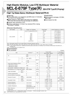
www.hitachi-chem.co.jpGeneral Characteristics Item Condition Unit UL ANSI Multilayer Materials Multilayer Materials Materials For ICT Infrastructure *1) Heating Rate: 10℃/min. *2) Measured by Triplate-line Resonator *3)Cavity Resomator *4) 0.1mm *5) 0.2mm …

認定状況について - hitachi-chem.co.jp
www.hitachi-chem.co.jpul規格 bs規格・csa規格 電気用品安全法(cmj登録制度) 認定状況について p96 p98 p99 95

第 37 号 平成13年7月 ... - hitachi-chem.co.jp
www.hitachi-chem.co.jp3 第 37 号 平成13年7月 テクニカルレポート 巻頭言 光の風(高分子光部品の時代へ)─────────────────────────────────────────5
60 2017 - hitachi-chem.co.jp
www.hitachi-chem.co.jp日立化成 テクニカルレポート Hitachi Chemical Technical Report 第60号/2017.12 巻頭言 エネルギー事業のグローバル展開 ─ビジネスパートナーの真のニーズを捉える─ 4
High Elastic Modulus, Low CTE ... - hitachi-chem.co.jp
www.hitachi-chem.co.jpCTE is 20% lower in X,Y directions and 50% lower in Z direction than that of our standard FR-4. Elastic modulus is 30% higher than that of our standard
Anti-Fingerprint UV Curable Hard Coatings - …
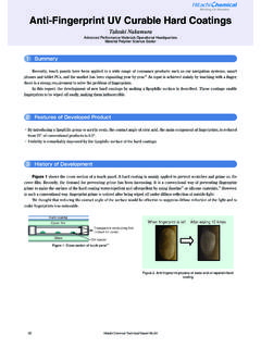
www.hitachi-chem.co.jp37 Hitachi Chemical Technical Report No.54 Recently, touch panels have been applied to a wide range of consumer products such as car navigation systems, smart phones and tablet PCs, and the market has been expanding year by year.

日立機能性アクリレート メタクリレート
www.hitachi-chem.co.jp2 ファンクリル(fancryl)は、日立化成が開発した機能性アクリレート、メタクリレートの商品名です。 fa- a、fa- mの末尾の「a」はアクリレートを、「m」はメタクリレートを示しています。
Related documents

8 章 WG7 実装 - JEITA半導体部会
semicon.jeita.or.jp半導体技術ロードマップ専門委員会 平成21 年度報告 ステムメモリの接続に使われている。ゲーム機器用途の CoC 接続を用いたSiP では200 Gbps のデータ転送レ
図2-4-1 主なIC用パッケージの種類
semicon.jeita.or.jp材 料 実装法 形状・リード方向 タイプ名 外 観 qfp tcp(tab) cob cot simm dimm 4方向リード モジュール(ソケットタイプ)
3D SiP(System-in-Package) 기술 동향 - :: DBguide.net
www.dbguide.net주간기술동향 통권 1367호 2008. 10. 8. 16 패키지 위에 패키지를 적층하는 PoP(Package-on-Package)로 구분된다[5]. MCP는 최소한의

Packaging Material System for Electronic Devices
www.hitachi-chem.co.jp日立化成テクニカルレポートNo.40(2003-1) 9 総 説 ルギーとして相対値で示すが,ダイパッドとの界面のせん断

3章 実装形態 - ieice-hbkb.org
www.ieice-hbkb.org10 群-3 編-3 章 〈ver.1/2010.2.1〉 10群 - 3編 - 3章 . 3-2 3次元実装技術と3次元SiP (執筆者:小谷光司)[2009年9月 受領] 前述のように,SiP とはMCP 技術を用いて複数の集積回路チップからなるシステムを単一

Terminology - ISSI
www.issi.com1940 Zanker Rd. • San Jose, CA. 95112 • Tel: 408.969.6600 • KGD@issi.com • www.issi.com Introduction Die-level customers require a memory partner who can meet their many unique needs for high quality, long term support,
How to Choose the Right DRAM for an Application …
www.issi.comHow to Choose the Right DRAM for an Application Pat Lasserre, Director, Strategic Marketing, Integrated Silicon Solution Inc. (ISSI) While price and density play large roles in selecting dynamic random access memory (DRAM), many other

Call for Papers - エレクトロニクス実装学会
www.jiep.or.jpCall for Papers 2018 International Conference on Electronics Packaging and IMAPS All Asia Conference Major Topics Advanced Packaging 2.5D/3D, Advanced CSP and POP, Advanced Flip-Chip, Automotive,