Transcription of MFRC522 Standard performance MIFARE and NTAG frontend …
1 1. IntroductionThis document describes the functionality and electrical specifications of the contactless reader/writer : The MFRC522 supports all variants of the MIFARE Mini, MIFARE 1K, MIFARE 4K, MIFARE Ultralight, MIFARE DESFire EV1 and MIFARE Plus RF identification protocols. To aid readability throughout this data sheet , the MIFARE Mini, MIFARE 1K, MIFARE 4K, MIFARE Ultralight, MIFARE DESFire EV1 and MIFARE Plus products and protocols have the generic name Differences between version and MFRC522 is available in two versions: MFRC52201HN1, hereafter referred to version and MFRC52202HN1, hereafter referred to version MFRC522 version is fully compatible to version and offers in addition the following features and improvements.
2 Increased stability of the reader IC in rough conditions An additional timer prescaler, see Section A corrected CRC handling when RX Multiple is set to 1 This data sheet version covers both versions of the MFRC522 and describes the differences between the versions if General descriptionThe MFRC522 is a highly integrated reader/writer IC for contactless communication at MHz. The MFRC522 reader supports ISO/IEC 14443 A/ MIFARE and MFRC522 s internal transmitter is able to drive a reader/writer antenna designed to communicate with ISO/IEC 14443 A/ MIFARE cards and transponders without additional active circuitry.
3 The receiver module provides a robust and efficient implementation for demodulating and decoding signals from ISO/IEC 14443 A/ MIFARE compatible cards and transponders. The digital module manages the complete ISO/IEC 14443 A framing and error detection (parity and CRC) MFRC522 supports MF1xxS20, MF1xxS70 and MF1xxS50 products. The MFRC522 supports contactless communication and uses MIFARE higher transfer speeds up to 848 kBd in both performance MIFARE and NTAG frontendRev. 27 April 2016112139 Product data sheetCOMPANY PUBLICMFRC522 All information provided in this document is subject to legal disclaimers.
4 NXP Semiconductors 2016. All rights data sheetCOMPANY PUBLICRev. 27 April 2016112139 2 of 95 NXP SemiconductorsMFRC522 Standard performance MIFARE and NTAG frontendThe following host interfaces are provided: Serial Peripheral Interface (SPI) Serial UART (similar to RS232 with voltage levels dependant on pin voltage supply) I2C-bus interface3. Features and benefits Highly integrated analog circuitry to demodulate and decode responses Buffered output drivers for connecting an antenna with the minimum number of external components Supports ISO/IEC 14443 A/ MIFARE and NTAG Typical operating distance in Read/Write mode up to 50 mm depending on the antenna size and tuning Supports MF1xxS20.
5 MF1xxS70 and MF1xxS50 encryption in Read/Write mode Supports ISO/IEC 14443 A higher transfer speed communication up to 848 kBd Supports MFIN/MFOUT Additional internal power supply to the smart card IC connected via MFIN/MFOUT Supported host interfaces SPI up to 10 Mbit/s I2C-bus interface up to 400 kBd in Fast mode, up to 3400 kBd in High-speed mode RS232 Serial UART up to kBd, with voltage levels dependant on pin voltage supply FIFO buffer handles 64 byte send and receive Flexible interrupt modes Hard reset with low power function Power-down by software mode Programmable timer Internal oscillator for connection to MHz quartz crystal V to V power supply CRC coprocessor Programmable I/O pins Internal self-test4.
6 Quick reference data Table reference dataSymbolParameterConditionsMinTypMaxUn itVDDA analog supply voltageVDD(PVDD) VDDA = VDDD = VDD(TVDD); VSSA=VSSD=VSS(PVSS)=VSS(TVSS)=0V[1][2] supply (TVDD)TVDD supply (PVDD)PVDD supply voltage[3] (SVDD)SVDD supply voltageVSSA=VSSD=VSS(PVSS)=VSS(TVSS)= 0 information provided in this document is subject to legal disclaimers. NXP Semiconductors 2016. All rights data sheetCOMPANY PUBLICRev. 27 April 2016112139 3 of 95 NXP SemiconductorsMFRC522 Standard performance MIFARE and NTAG frontend [1]Supply voltages below 3 V reduce the performance in, for example, the achievable operating distance.
7 [2]VDDA, VDDD and VDD(TVDD) must always be the same voltage.[3]VDD(PVDD) must always be the same or lower voltage than VDDD.[4]Ipd is the total current for all supplies.[5]IDD(PVDD) depends on the overall load at the digital pins.[6]IDD(TVDD) depends on VDD(TVDD) and the external circuit connected to pins TX1 and TX2.[7]During typical circuit operation, the overall current is below 100 mA.[8]Typical value using a complementary driver configuration and an antenna matched to 40 between pins TX1 and TX2 at MHz. 5. Ordering information [1]Delivered in one tray.[2]Delivered in five currentVDDA=VDDD= VDD(TVDD) =VDD(PVDD) =3 Vhard power-down; pin NRSTPD set LOW[4]--5 Asoft power-down; RF level detector on[4]--10 AIDDD digital supply currentpin DVDD; VDDD= supply currentpin AVDD; VDDA= 3 V, CommandReg register s RcvOff bit = 0-710mApin AVDD; receiver switched off; VDDA=3V, CommandReg register s RcvOff bit = 1-35mAIDD(PVDD)PVDD supply currentpin PVDD[5]--40mAIDD(TVDD)TVDD supply currentpin TVDD; continuous wave[6][7][8]-60100mATambambient temperatureHVQFN32 25-+85 CTable reference data .
8 ContinuedSymbolParameterConditionsMinTyp MaxUnitTable informationType numberPackageNameDescriptionVersionMFRC5 2201HN1/TRAYB[1]HVQFN32 plastic thermal enhanced very thin quad flat package; no leads; 32 terminal; body 5 5 mmSOT617-1 MFRC52201HN1/TRAYBM[2]HVQFN32 plastic thermal enhanced very thin quad flat package; no leads; 32 terminal; body 5 5 mmSOT617-1 MFRC52202HN1/TRAYB[1]HVQFN32 plastic thermal enhanced very thin quad flat package; no leads; 32 terminal; body 5 5 mmSOT617-1 MFRC52202HN1/TRAYBM[2]HVQFN32 plastic thermal enhanced very thin quad flat package; no leads; 32 terminal; body 5 5 mmSOT617-1 MFRC522 All information provided in this document is subject to legal disclaimers.
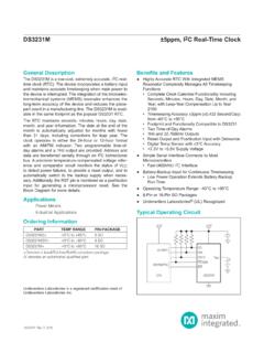
9 NXP Semiconductors 2016. All rights data sheetCOMPANY PUBLICRev. 27 April 2016112139 4 of 95 NXP SemiconductorsMFRC522 Standard performance MIFARE and NTAG frontend6. Block diagramThe analog interface handles the modulation and demodulation of the analog contactless UART manages the protocol requirements for the communication protocols in cooperation with the host. The FIFO buffer ensures fast and convenient data transfer to and from the host and the contactless UART and vice host interfaces are implemented to meet different customer requirements. Fig block diagram of the MFRC522001aaj627 HOSTANTENNAFIFOBUFFERANALOGINTERFACECONT ACTLESSUARTSERIAL UARTSPII2C-BUSREGISTER BANKMFRC522 All information provided in this document is subject to legal disclaimers.
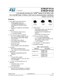
10 NXP Semiconductors 2016. All rights data sheetCOMPANY PUBLICRev. 27 April 2016112139 5 of 95 NXP SemiconductorsMFRC522 Standard performance MIFARE and NTAG frontend Fig block diagram of the MFRC522001aak602 DVDDNRSTPDIRQMFINMFOUTSVDDOSCINOSCOUTVMI D AUX1 AUX2 RXTVSSTX1TX2 TVDD1619201710, 14111312 DVSSAVDDPVSSPVDDSDA/NSS/RXEAI2C5224321D1 /ADR_525D2/ADR_426D3/ADR_327D4/ADR_228D5 /ADR_1/SCK/DTRQ29D6/ADR_0/MOSI/MX30D7/SC L/MISO/TX31 AVSS3623789212241518 FIFO CONTROLMIFARE CLASSIC UNITSTATE MACHINECOMMAND REGISTERPROGRAMABLE TIMERINTERRUPT CONTROLCRC16 GENERATION AND CHECKPARALLEL/SERIALCONVERTERSERIAL data SWITCHTRANSMITTER CONTROLBIT COUNTERPARITY GENERATION AND CHECKFRAME GENERATION AND CHECKBIT DECODINGBIT ENCODINGRANDOM NUMBERGENERATORANALOG TO DIGITALCONVERTERI-CHANNELAMPLIFIERANALOG TESTMULTIPLEXORANDDIGITAL