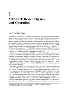
Transcription of MOS TRANSISTOR REVIEW - Stanford University
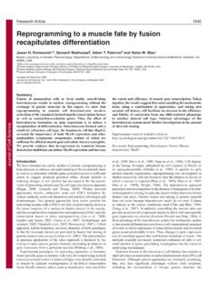
1 EE 316 / Prof. SaraswatHandout 5 MOS TRANSISTOR REVIEW3D band diagram of a long channel enhancement mode NMOS transistorVG = VD = 0VG > VTVD > 0VG > 0VD = 0EE 616 / +N+V (+) D+VDGPN+N+V (+) D+VD (small)GInversionLayerDepletionRegionDPN +N+V V > VGInversion layer ends IDVDIDVDIDVDDPN+N+V V = VGInversion layerpinches offDSATIDVDDSATMOS Transistor3 From EE216 notes:Drain currentIJ dydzWQE dyDxInx== Charge density in the channel:QI(y)= CoxVG VT(y)[]Gate voltage required to induce inversion under the influence of VDVT(y)=VFB+1 Cox2 sqNa 2 p VB V(y)()[] 2 p+V(y)Solving the above 3 equations we get ID VD characteristicsLinear RegionID=WL n CoxVG VT[]VDSaturation RegionIDSAT W2L n oxtoxVG VT()2 EE 616 / Device ScalingNaPN+N+LxoxXjolPN+N+SGDS caled MOS TransistorWhy do we scale MOS transistors?
2 1. Increase device packing density2. Improve frequency response (transit time) 1L3. Improve current drive (transconductance gm)gIVVconstWLKtVVlinear regionWLKtVVVsaturation regionmDGDnoxoxDDnoxoxGTDSATSAT== < ()> for Vfor VDD,,Decreasing the channel length and gate oxide thickness increases gm, , the currentdrive of the TRANSISTOR . Much of the scaling is therefore driven by decrease in L and if only these two parameters are scaled many problems are encountered, ,increased electric 1974 Dennard proposed a scaling methodology which maintains the electric field inthe device constant. (Dennard et al., IEEE JSSCC, 9, pp. 256-268, 1974)Device/Circuit Parameter Constant Field Scaling FactorDimension :xox, L, W, Xj,1/KSubstrate doping :NaKSupply voltage :V1/KSupply current :I1/KGate Capacitance :W L/xox1/KGate delay :C V / I1/KPower dissipation :C V2 / delay1/K2 MOS Transistor5In reality constant field scaling has not been observed strictly.
3 Since the transistorcurrent is proportional to the gate overdrive (VG-VT), high performance demands havedictated the use of higher supply voltage. However, higher supply voltage impliesincreased power dissipation (CV2f). In the recent past low power applications havebecome important and have required a scaling scenario with lower supply length ( m) oxide (nm) depth ( m)> supply - : Davri, et al. Proc. IEEE, April 1995 Device/Circuit Parameter Quasi Constant Voltage Scaling (K>B>1)Dimension :L, W, xox, Xj,1/KSubstrate doping :NKSupply voltage :V1/BEE 616 / of Scaled MOSFETE ffect of Reducing Channel Length: Drain Induced Barrier Lowering (DIBL)In devices with long channel lengths, the gate is completely responsible for depletingthe semiconductor (QB).
4 In very short channel devices, part of the depletion isaccomplished by the drain and source biasSince less gate voltage is required to deplete QB, VT as L . Similarly, as VD , moreQB is depleted by the drain bias, and hence VT . These effects are particularlypronounced in lightly doped depletedby sourceQ depletedby drainBBN+ sourceN+ drainGateP-SiDepletion regionIf the channel length becomes too short, the depletion region from the drain can reachthe source side and reduces the barrier for electron injection. This is known as + sourceN+ drainGateDepletion-region boundariesDirect carrier injectionIn devices with long channel lengths, the gate is completely responsible for depletingthe semiconductor (QB).
5 In very short channel devices, part of the depletion isaccomplished by the drain and source bias. Since less gate voltage is required toMOS Transistor7deplete QB, the barrier for electron injection from source to drain decreases. This isknown as drain induced barrier lowering (DIBL).Potential variation along the channel illustrating drain induced barrier lowering (DIBL).DIBL results in an increase in drain current at a given VG. Therefore VT as L .Similarly, as VD , more QB is depleted by the drain bias, and hence ID and VT .Effect of drain induced barrier lowering on drain 616 / Mobility: Velocity SaturationThe mobility of the carriers reduces at higher electric fields normally encountered insmall channel length devices due to velocity saturation as a function of electric fieldAs the channel length, L, is reduced while the supply voltage is not, the tangentialelectric field will increase, and the carrier velocity may saturate.
6 C 104 V/cm forelectrons. Hence for N-channel MOSFET with L < 1 m, velocity saturation causesthe channel current to reach saturation before VD = VG - VT. Instead of IDSAT being proportional (VG -VT)2 it is linearly proportional to (VG -VT) and isapproximately given byIWC(VV)vDsatoxGTsat= MOS Transistor9ec 5 104 V/cm for holes, hence velocity saturation for P-channel MOSFET will notbecome important until L < Effects of velocity saturation on the MOSFET I-V characteristics.(a)Experimental characteristics of a MOSFET with L = m, x0 = m,Comparative theoretical characteristics computed (b) including velocity saturation and(c) ignoring velocity ConductionWhen the surface is in weak inversion ( , o < s < - p, VG < VT), a conductingchannel starts to form and a low level of current flows between source and mv/decadeS < 60 mv/decade VTIDVG60 mv/decadeS < 60 mv/decade IDIDVG60 mv/decadeS < 60 mv/decade 60 mv/decadeS < 60 mv/decade VTVT VGSIDVTS ubthresholdcurrentIdealEE 616 / MOS subthreshold slope S is limited to kT/q (60mV/dec)
7 ID leakage Static power Circuit instability VDD is scaled for low power,delay, VT must scale to maintain ID (ON)With subthreshold slope limited to 60mv/decade the dynamic range becomes Carrier EffectsFrom our p-n junction discussion we remember that the maximum electric field intensityis near the junction itself and it increases with the reverse bias. max()= 2qNVaiDoxIn the case of MOS TRANSISTOR the maximum electric field is near the drain-substratejunction. The drain reverse bias has to be dropped from drain to source. As the channellength is reduced the electric field intensity in the channel near the drain increases morerapidly in comparison to the long channel case as i does not Transistor11 The free carriers passing through the high-field can gain sufficient energy to causeseveral hot-carrier effects.
8 This can cause many serious problems for the carriers can have sufficient energy to overcome the oxide-Si barrier. They areinjected from channel to the gate oxide (process 1) and cause gate current to of some of this charge can change VT permanently. Avalanching can takeplace producing electron-hole pairs (process 2). The holes produced by avalanchingdrift into the substrate and are collected by the substrate contact (process 3) causingIsub IR drop due to Isub(process 4) can cause substrate-source junction to be forwardbiased causing electrons to be injected from source into substrate (process 5). Some ofthe injected electrons are collected by the reversed biased drain and cause a parasiticbipolar action (process 5).
9 EE 616 / Oxide Degradation and BreakdowneCathodeOxideAnodeh(1)(2)(4)(5) (6)Hydrogeneeh(1) Electron injection(2) Energy released by hot electron(3) Bond breaking at the interface - trap generation(4) Hot hole generation by impact ionization and injection(5) Energy released by hot hole - trap generation(6) Hydrogen release - trap generation(3)(3)Ref: Apte & Saraswat IEEE Trans. Electron Dev., Sept 1994 Damage initiationDamage propagationBreakdownDamage clusterSiO2 AnodeCathodeBreakdown field ~ 8 MV/cm for thick oxides and increases > 10 MV/cm for Transistor13 Band-to-Band TunnelingFor small gate bias at high drain bias a significant drain leakage can be observed,especially for short channel electric field can be very high in the drain region for VD high and VG = 0.
10 Thiscan cause band-to-band tunneling. This will happen only if the electric field is sufficientlyhigh to cause large band figure below shows band-to-band tunnelingEE 616 / of Reducing Channel Width on VTThere are no diffusions on the side of the channel. Hence the depletion region extendssideways in areas lying outside the gate controlled region increasing the apparentchannel width. As a result the VT is increased. Note that the effect here is opposite tothat of reducing channel View of the MOS transistoreGateVTW