Example: stock market
MOSFET transistor I-V characteristics
Depletion Mode NMOSFET • Depletion mode FETs have a channel implanted such that there is conduction with V GS=0 • The operation is the same as the enhancement mode FET, but the threshold voltage is shifted •Vt is negative for depletion NMOS, and positive for depletion PMOS VGS n+ n+ VS VDS n+ p
Tags:
Information
Domain:
Source:
Link to this page:
Documents from same domain
Computer Architecture: Dataflow (Part I)
course.ece.cmu.eduComputer Architecture,” ACM Computing Surveys 1982. ! Veen, “Dataflow Machine Architecture,” ACM Computing Surveys 1986. ! Gurd et al., “The Manchester prototype dataflow computer,” CACM 1985. ! Arvind and Nikhil, “Executing a Program on the MIT Tagged-Token Dataflow Architecture,” IEEE TC 1990. !

Computer Architecture: Vector Processing: SIMD/Vector/GPU ...
course.ece.cmu.eduCarnegie Mellon University Vector Processing: Exploiting Regular (Data) Parallelism Data Parallelism Concurrency arises from performing the same operations on different pieces of data Single instruction multiple data (SIMD) E.g., dot product of two vectors Contrast with data flow

Computer Architecture: Branch Prediction
course.ece.cmu.eduHow to Handle Control Dependences Critical to keep the pipeline full with correct sequence of dynamic instructions. Potential solutions if the instruction is a control-flow instruction: Stall the pipeline until we know the next fetch address Guess the next fetch address (branch prediction) Employ delayed branching (branch delay slot) Do something else (fine-grained multithreading)

Computer Architecture: Main Memory (Part I)
course.ece.cmu.eduMemory Bank Organization and Operation Read access sequence: 1. Decode row address & drive word-lines 2. Selected bits drive bit-lines • Entire row read 3. Amplify row data 4. Decode column address & select subset of row • Send to output 5. …

CMOS Power Consumption - ECE:Course Page
course.ece.cmu.eduWays to reducing power consumption Load capacitance (C L) ⌧Roughly proportional to the chip area Switching activity (avg. number of transitions/cycle) ⌧Very data dependent ⌧A big portion due to glitches (real-delay) Clock frequency (f) ⌧Lowering only f decreases average power, but total energy is the same and throughput is worse 1.00 1 ...

HDL Compiler for Verilog Reference Manual
course.ece.cmu.eduComments? E-mail your comments about Synopsys documentation to doc@synopsys.com HDL Compiler for Verilog Reference Manual Version 2000.05, May 2000

Computer Architecture: Multithreading
course.ece.cmu.eduSun Niagara Multithreaded Pipeline 13 Tera MTA Fine-grained Multithreading 256 processors, each with a 21-cycle pipeline 128 active threads A thread can issue instructions every 21 cycles Then, why 128 threads? Memory latency: approximately 150 cycles No data cache Threads can be blocked waiting for memory More threads better ability to tolerate memory latency

A Primer on Memory Consistency and Cache Coherence
course.ece.cmu.eduDaniel J. Sorin, Duke University Mark D. Hill and David A. Wood, University of Wisconsin, Madison ... We thank Blake Hechtman for implementing and testing (and debugging!) all of the coherence protocols in this primer. As the reader will soon …
Related documents

An introduction to Depletion-mode MOSFETs
aldinc.comdealing with depletion-mode MOSFETs will be straightforward. A few characteristics that may be a bit confusing are: 1. Drain saturation current - IDSS With an enhancement-mode MOSFET this is a leakage current. With a depletion-mode MOSFET it is the maximum limiting current that can flow between the drain and
TEORI DASAR MOSFET - Universitas Brawijaya
maulana.lecture.ub.ac.idGambar 1 Simbol Transistor MOSFET Mode Depletion (a). N-Channel Depletion (b). P-Channel Depletion 2) Transistor Mode peningkatan (Transistor Mode Enhancement) Transistor mode enhancement ini pada fisiknya tidak memiliki saluran antara drain dan sourcenya karena lapisan bulk meluas dengan lapisan SiO ...
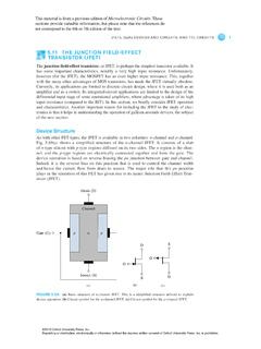
5.11 THE JUNCTION FIELD-EFFECT TRANSISTOR (JFET)
global.oup.comThe description above clearly indicates that the JFET is a depletion-type device. Its char-acteristics should therefore be similar to those of the depletion-type MOSFET. This is true with a very important exception: While it is possible to operate the depletion-type MOSFET in the enhancement mode (by simply applying a positive v GS if the ...
Field Effect Transistors in Theory and Practice ...
www.nxp.comMOSFET. A depletion-type MOSFET can be made in the following manner: Starting with the basic structure of Figure 4, a moderate resistivity n-channel is diffused between the source and drain so that drain current can flow when the gate potential is at zero volts (Figure 7). In this manner, the MOSFET can be made to exhibit depletion characteristics.

Chapter 9: FET Amplifiers And Switching Circuits
staff-old.najah.eduWhen Vgs < 0 Æthe depletion mode, and Id decreases. When Vgs > 0 Æthe enhancement mode, and Id increases At VGS = 0 ÆID = IDSS ÆVD = VDS can be calculated The ac analysis is the same as for the JFET amplifier. 9-1: The Common Source Amplifier E-MOSFET Amplifier Operation: A voltage divider common-source amplifier for n-channel E-MOSFET is ...

Design And Application Guide For High Speed MOSFET Gate ...
www.radio-sensors.seMOSFET. The most important parasitic components influencing switching performance are shown in this model. Their respective roles will be discussed in the next chapter which is dedicated to the switching procedure of the device. MOSFET Critical Parameters When switch mode operation of the MOSFET is considered, the goal is to switch between the
MOS TRANSISTOR REVIEW - Stanford University
web.stanford.eduLimitations of Scaled MOSFET Effect of Reducing Channel Length: Drain Induced Barrier Lowering (DIBL) In devices with long channel lengths, the gate is completely responsible for depleting the semiconductor (QB). In very short channel devices, part of the depletion is accomplished by the drain and source bias
MOSFET Device Physics and Operation
homepages.rpi.edu6 MOSFET DEVICE PHYSICS AND OPERATION Using Gauss’ law, we can relate the total charge Q s per unit area (carrier charge and depletion charge) in the semiconductor to the surface electric field by Q s =−ε sF s.(1.12) At the flat-band condition (V = VFB), the surface charge is equal to zero.In accumulation