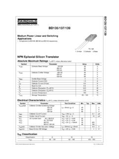
Transcription of MPSA18 NPN General Purpose Amplifier - redrok.com
1 MPSA18 Discrete POWER & SignalTechnologiesNPN General Purpose AmplifierMPSA18 This device is designed for low noise, high gain, applications atcollector currents from 1 A to 50 mA. Sourced from Process07. See 2N5088 for Maximum Ratings* TA = 25 C unless otherwise noted*These ratings are limiting values above which the serviceability of any semiconductor device may be :1) These ratings are based on a maximum junction temperature of 150 degrees ) These are steady state limits. The factory should be consulted on applications involving pulsed or low duty cycle Characteristics TA = 25 C unless otherwise noted SymbolParameterValueUnitsVCEOC ollector-Emitter Voltage45 VVCBOC ollector- Bas e Volt age45 VVEBOE mitt er-Base Vol Current - Continuous100mATJ, TstgOper ating and St orage J uncti on Temperat ure Range-55 to +150 CSymbolCharacteristicMaxUnitsMPSA18 PDTotal Device DissipationD erate above 25 CR JCThermal Resist anc e, J uncti on to Case83.
2 3 C/WR JAThermal Resist anc e, J uncti on to Ambient200 C/WCBETO-92 1997 Fairchild Semiconductor CorporationMPSA18 NPN General Purpose Amplifier (continued)Electrical Characteristics TA = 25 C unless otherwise notedOFF CHARACTERISTICSS ymbolParameterTest ConditionsMinMaxUnitsV(BR) CEOC oll ector -Emitt er Breakdow n Vol tage*IC = 10 mA, IB = 045VV(BR) CBOC oll ector -Base Br eakdown Vol tageIC = 100 A, IE = 045VV(BR) EBOE mitt er-Base Breakdown Volt ageIE = 10 A, IC = Cutoff CurrentVCB = 30 V, IE = 050nAON CHARACTERISTICS*hFEDC Current GainVCE = 5. 0 V, IC = 10 AVCE = 5.
3 0 V, IC = 100 AVCE = 5. 0 V, IC = 1. 0 mAVCE = 5. 0 V, IC = 10 mA4005005005001500 VCE(sat)Collector-Emitter Saturation VoltageIC = 10 mA, IB = 0. 5 mAIC = 50 mA, IB = 5. 0 (on)Base-Emitter On VoltageVCE = 5. 0 V, IC = 1. 0 SIGNAL CHARACTERISTICSCcbC ollector -Base C apacit anceVCB = 5. 0 V, f = 1. 0 er-Base Capac itanceVEB = 0. 5 V, f = 1. 0 Gain - Bandwidth ProductIC = 1. 0 mA, VCE = 5. 0 V,f = 100 MHz100 MHzNFNoise FigureVCE = 5. 0 V, IC = 100 A,RS = 10 k , f = 1. 0 kH z, *Pulse Test: Pulse Width 300 s, Duty Cycle Tape and Reel DataMarch 2001, Rev.
4 B1 2001 Fairchild Semiconductor CorporationTO-92 PackagingConfiguration: Figure PACK OPTIONSee Fig for 2 AmmoPack Options2000 units perEO70 box for std optionFSCINT Label530mm x 130mm x 83mmIntermediate box10,000 units maximumper intermediate boxfor std optionFSCINT Label114mm x 102mm x 51mmImmediate BoxAnti-static Bubble Sheets(TO-92) BULK PACKING INFORMATIONEOLCODEDESCRIPTIONLEADCLIPDIM ENSIONQUANTITYJ18 ZTO-18 OPTION STDNO LEAD K / BOXJ05 ZTO-5 OPTION STDNO LEAD K / BOXNO EOLCODETO-92 STANDARDSTRAIGHT FOR: PKG 92,NO K / BOXBULK OPTIONSee Bulk PackingInformation table375mm x 267mm x 375mmIntermediate BoxFSCINTL abelCustomizedLabel333mm x 231mm x 183mmIntermediate BoxFSCINTL abelCustomizedLabelTO-92 TNR/AMMO PACKING INFROMATIONP ackingStyleQuantityEOL codeReelA2,000D26ZE2,000 D27 ZAmmoM2,000D74ZP2,000 D75 ZUnit weight = gmReel weight with components = kgAmmo weight with components = kgMax quantity per intermediate box = 10.
5 000 unitsF63 TNRL abel5 Ammo boxes per Intermediate BoxCustomizedLabel327mm x 158mm x 135mmImmediate BoxLOT: CBVK741B019 NSID: PN2222ND/C1: D9842 SPEC REV: B2 SPEC: QTY: 10000QA REV:FAIRCHILD SEMICONDUCTOR CORPORATION HTB:B(FSCINT)F63 TNRL abelCustomizedLabel5 Reels perIntermediate BoxTAPE and REEL OPTIONSee Fig for variousReeling StylesLOT: CBVK741B019 FSID: PN222ND/C1: D9842 QTY1: SPEC REV: SPEC:QTY: 2000D/C2: QTY2: CPN:N/F: F (F63 TNR)3F63 TNR Label sampleFSCINT Label sampleC5 EO70 boxes per intermediate BoxustomizedLabel 94 (NON PROELECTRON SERIES), 96L34 ZTO-92 STANDARDSTRAIGHT FOR: PKG 94NO K / BOX(PROELECTRON SERIES BCXXX, BFXXX, BSRXXX),97, 98TO-92 Tape and Reel Data, continuedSeptember 1999, Rev.
6 BTO-92 Reeling StyleConfiguration: Figure A , D26Z, D70Z (s/h)Machine Option A (H)Style E , D27Z, D71Z (s/h)Machine Option E (J)FIRST WIRE OFF IS EMITTERADHESIVE TAPE IS ON THE TOP SIDEFLAT OF TRANSISTOR IS ON BOTTOM ORDER STYLED75Z (P)FIRST WIRE OFF IS COLLECTORADHESIVE TAPE IS ON THE TOP SIDEFLAT OF TRANSISTOR IS ON TOP ORDER STYLED74Z (M)TO-92 Radial Ammo PackagingConfiguration: Figure WIRE OFF IS EMITTER (ON PKG. 92)ADHESIVE TAPE IS ON BOTTOM SIDEFLAT OF TRANSISTOR IS ON BOTTOMFIRST WIRE OFF IS COLLECTOR (ON PKG. 92)ADHESIVE TAPE IS ON BOTTOM SIDEFLAT OF TRANSISTOR IS ON TOPITEM DESCRIPTIONBase of Package to Lead BendComponent HeightLead Clinch Height Component Base HeightComponent Alignment ( side/side )Component Alignment ( front/back )Component PitchFeed Hole PitchHole Center to First LeadHole Center to Component CenterLead SpreadLead ThicknessCut Lead LengthTaped Lead LengthTaped Lead ThicknessCarrier Tape ThicknessCarrier Tape WidthHold - down Tape WidthHold - down Tape positionFeed Hole PositionSprocket Hole DiameterLead Spring OutSYMBOLbHaHOH1 PdHdPPOP1P2F1 (max) (+/- )
7 (+/- ) (+/- ) (max) (max) (+/- ) (+/- ) (+ , ) (+/- ) (+/- 0 .010) (+ , ) (max) (+ , ) (+/- ) (+/- ) (+ , ) (+/- ) (max) (+/- ) (+ , ) (max)Note : All dimensions are in DESCRIPTIONSYSMBOLMINIMUMMAXIMUMReel Hole Diameter (Standard) (Small Hole) Recess Inner Recess to Flange Inner to Hub Center : All dimensions are inchesTO-92 Tape and Reel TapingDimension Configuration: Figure F1 DOPPdbdL1 LSWOW2 Wtt1 HdW1TO-92 ReelConfiguration: Figure Direction of FeedSENSITIVE DEVICESELECTROSTATICD1D3 Customized LabelW2W1W3F63 TNR LabelD4D2TO-92 Tape and Reel Data, continuedJuly 1999, Rev.
8 ATO-92 (FS PKG Code 92, 94, 96)TO-92 Package DimensionsJanuary 2000, Rev. B1:1 Scale 1:1 on letter size paperDimensions shown below are in:inches [millimeters]Part Weight per unit (gram): 2000 Fairchild Semiconductor InternationalTRADEMARKSThe following are registered and unregistered trademarks Fairchild Semiconductor owns or is authorized to use and isnot intended to be an exhaustive list of all such SUPPORT POLICYFAIRCHILD S PRODUCTS ARE NOT AUTHORIZED FOR USE AS CRITICAL COMPONENTS IN LIFE SUPPORTDEVICES OR SYSTEMS WITHOUT THE EXPRESS WRITTEN APPROVAL OF FAIRCHILD SEMICONDUCTOR used herein:1.
9 Life support devices or systems are devices orsystems which, (a) are intended for surgical implant intothe body, or (b) support or sustain life, or (c) whosefailure to perform when properly used in accordancewith instructions for use provided in the labeling, can bereasonably expected to result in significant injury to A critical component is any component of a lifesupport device or system whose failure to perform canbe reasonably expected to cause the failure of the lifesupport device or system, or to affect its safety STATUS DEFINITIONSD efinition of TermsDatasheet IdentificationProduct StatusDefinitionAdvance InformationPreliminaryNo Identification NeededObsoleteThis datasheet contains the design specifications forproduct development.
10 Specifications may change inany manner without datasheet contains preliminary data, andsupplementary data will be published at a later Semiconductor reserves the right to makechanges at any time without notice in order to datasheet contains final specifications. FairchildSemiconductor reserves the right to make changes atany time without notice in order to improve datasheet contains specifications on a productthat has been discontinued by Fairchild datasheet is printed for reference information orIn DesignFirst ProductionFull ProductionNot In ProductionDISCLAIMERFAIRCHILD SEMICONDUCTOR RESERVES THE RIGHT TO MAKE CHANGES WITHOUT FURTHERNOTICE TO ANY PRODUCTS HEREIN TO IMPROVE RELIABILITY, FUNCTION OR DESIGN.