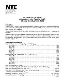
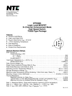
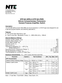
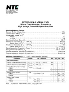
Transcription of NTE957 Integrated Circuit 3–Terminal Adjustable …
1 NTE957 Integrated Circuit3 terminal Adjustable NegativeVoltage RegulatorDescription:The NTE957 is an Adjustable 3 terminal negative voltage regulator in a TO220 type package capableof supplying in excess of over a to 37V output range. The Circuit design has been optimizedfor excellent regulation and low thermal transients. Further, the NTE957 features internal current limiting,thermal shutdown, and safe area compensation, making this device virtually blowout proof NTE957 serves a wide variety of applications including local on card regulation, programmable output voltage regulation or precision current regulation.
2 The NTE957 is the ideal complement to theNTE956 Adjustable positive :DOutput voltage Adjustable from to 37 VDGuaranteed Output CurrentDLine Regulation Typically Regulation Typically Thermal Regulation: Ripple RejectionDTemperature Independent Current LimitDInternal Thermal Overload ProtectionD100% Electrical Burn InDEliminates the Need to Stock Many VoltagesAbsolute Maximum Ratings:Power Dissipation, PDInternally Limited.. Input Output voltage Differential, VI VO40V.. Operating Junction Temperature Range, TJ0 to +125 C.
3 Storage Temperature Range, Tstg 65 to +150 C.. Typical Thermal Resistance, Junction to Case, RthJC4 C/W.. Lead Temperature (During Soldering, 10sec), TL+300 C.. Electrical Characteristics:(0 TJ +125 C, VIN VOUT = 5V, IO = 500mA, IMAX = , Note 1unless otherwise specified)ParameterSymbolTest ConditionsMinTypMaxUnitLine RegulationReglineTA = +25 C, 3V (VIN VOUT) 40V, Note 2 (VIN VOUT) 40V RegulationRegloadTA = +25 C, 10mA IO IMAX,VOUT 5V 1550mVNote 2 VOUT 5V IO 1 MAX, Note 2 VOUT 5V 2070mVVOUT 5V RegulationTA = +25 C, 20ms Pulse Pin CurrentIAdj 65100 AAdjustment Pin CurrentChange IAdj10mA IL IMAX, (VIN VOUT)
4 40V,TA = +25 C 25 AReference VoltageVrefTA = +25 C (VIN VOUT) 40V, 10mA IO 1 MAX,P PMAX StabilityTS0 TJ +125 C %Minimum Load CurrentILmin(VIN VOUT) 40V (VIN VOUT) 10V Output CurrentImaxVIN VOUT ALimitVIN VOUT = 40V ARMS Output Noise,% of VOUTNTA = +25 C, 10Hz f 10kHz %Ripple Rejection RatioRRVOUT = 10V, f = 120Hz 60 dBCADJ = 10 F6677 dBLong Term StabilitySTA = +125 C, 1000 Hours 1. Although power dissipation is internally limited, these specifications are applicable for powerdissipations of 2.
5 Regulation is measured at constant junction temperature, using pulse testing with a low dutycycle. Changes in output voltage due to heating effects are covered under the specificationfor thermal ( ) ( ) ( ) ( ) ( )Dia ( ) ( ) ( )